ALLPCB


Lead-free hot air solder leveling, commonly known as lead-free HASL, serves as a widely adopted surface finish in printed circuit board manufacturing. This process applies a thin layer of lead-free solder alloy to exposed copper pads and traces, providing both solderability and protection against oxidation. It meets environmental regulations that restrict hazardous substances while maintaining compatibility with subsequent assembly operations. Engineers and manufacturers rely on it for its balance of cost-effectiveness and performance in many standard applications. The shift from traditional tin-lead HASL to lead-free versions reflects broader industry efforts to reduce lead content below 0.1 percent by weight.
Why Lead-Free HASL Matters in Modern PCB Manufacturing
Lead-free HASL delivers a reliable surface finish that supports high-volume production while complying with global restrictions on lead in electronics. It forms a protective coating that preserves copper surfaces during storage and handling before assembly. Compared with other finishes, it offers good solderability at a relatively low cost, making it suitable for consumer electronics, industrial controls, and automotive boards where fine-pitch components are not required. The process integrates directly into existing manufacturing lines with appropriate adjustments for higher operating temperatures. Its durability under typical storage conditions supports shelf lives of six to twelve months when handled properly.
Technical Principles Behind the Lead-Free HASL Process
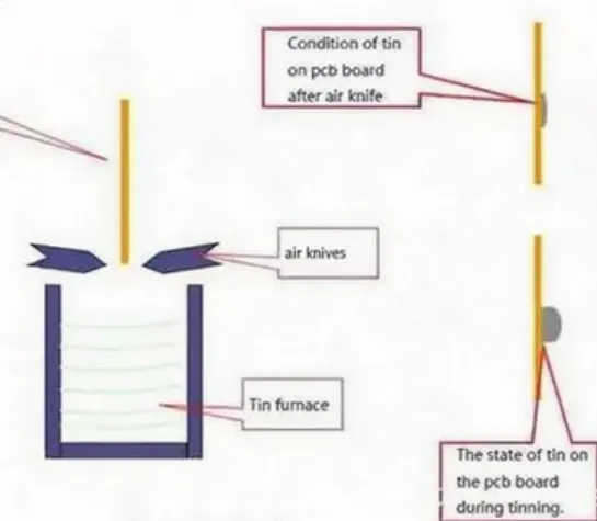
The lead-free HASL process relies on the wetting behavior of molten solder alloys on copper surfaces. Common alloys include tin-silver-copper compositions with melting points around 217 to 220 degrees Celsius and tin-copper alloys near 227 degrees Celsius. These higher melting points compared with traditional tin-lead solders necessitate elevated process temperatures to achieve proper flow and coverage. Hot air knives then remove excess solder while the board moves through the system, leaving a uniform coating typically thinner than that produced with leaded alloys due to differences in surface tension. Intermetallic compound formation occurs at the solder-copper interface during immersion, which influences long-term solderability if the coating becomes too thin or oxidized. Temperature control remains critical because the process window narrows significantly at these elevated levels, requiring precise monitoring to avoid thermal damage to the substrate or excessive intermetallic growth.
Flux plays an essential role by removing oxides and promoting wetting without introducing defects. Selection focuses on formulations compatible with the specific alloy and capable of withstanding preheat and immersion conditions. Inadequate flux activity can result in incomplete coverage or dewetting, while overly aggressive types may leave residues that affect downstream processes. Cooling rates after leveling also affect the final surface appearance and microstructure, with controlled air cooling often preferred for smoothness.
Step-by-Step Guide to the Lead-Free HASL Process
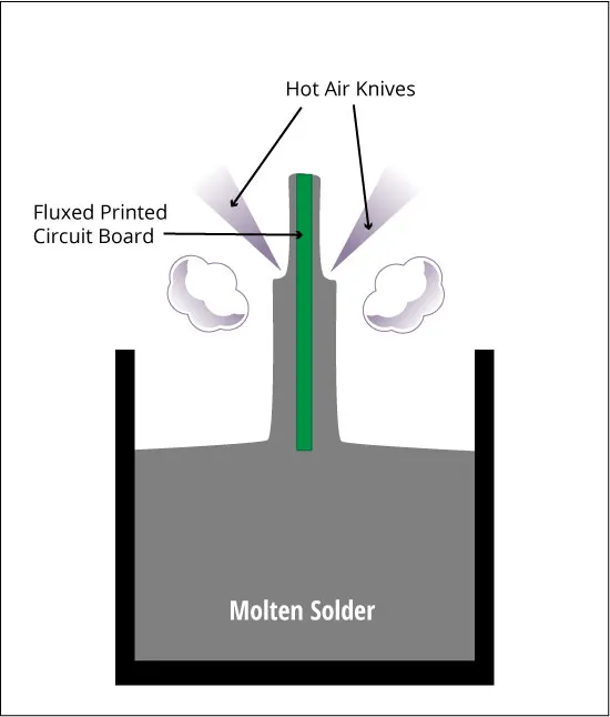
The lead-free HASL sequence begins with thorough cleaning of the PCB to remove contaminants from prior fabrication steps. Panels then receive a uniform application of flux, often through spraying or dipping, followed by preheating to activate the flux and minimize thermal shock upon immersion. The board enters a bath of molten lead-free solder maintained at temperatures typically between 240 and 255 degrees Celsius, with dwell times around two to three seconds depending on board thickness and design.
Excess solder is immediately stripped by hot air knives positioned above and below the panel, which operate at temperatures above the alloy melting point to ensure smooth leveling across pads, traces, and through-holes. Vertical systems handle panels on racks that move through the bath and knives, while horizontal configurations use rollers and nozzles for continuous processing. After leveling, the boards cool under controlled conditions to solidify the coating evenly. A subsequent washing stage removes flux residues, followed by drying to prepare the boards for inspection and further handling.
Temperature control throughout requires calibrated sensors and feedback systems to maintain consistency within narrow tolerances. Flux selection emphasizes compatibility with lead-free alloys, often favoring water-soluble or no-clean types that provide strong oxide removal without excessive charring at higher temperatures. Operators monitor parameters such as solder pot chemistry, air knife pressure, and conveyor speed to achieve consistent coating thickness and coplanarity suitable for component placement.
Best Practices for Temperature Control and Flux Selection
Maintaining stable solder bath temperatures prevents defects such as incomplete wetting or excessive copper dissolution. Preheat zones typically reach 150 to 160 degrees Celsius to reduce the temperature differential upon contact with the molten alloy. Air knife settings must balance solder removal with retention of adequate thickness on all features, particularly in fine-pitch areas or high-aspect-ratio holes. Regular analysis of the solder pot composition helps sustain alloy integrity over extended production runs.
Flux choice depends on board complexity, storage requirements, and assembly compatibility. Formulations with enhanced activity support the reduced wetting speed of lead-free alloys while minimizing residue that could interfere with automated optical inspection or conformal coating. Process validation often includes cross-section analysis to verify coating thickness and intermetallic layer quality against established acceptability criteria. Boards with thin substrates or dense copper areas may require adjusted parameters to limit warpage or thermal stress.
Quality Considerations and Process Optimization
Consistent results depend on integration with upstream and downstream manufacturing controls. Incoming material inspection ensures laminate and copper quality can withstand the thermal profile. Post-process verification commonly includes visual examination, thickness measurement via X-ray fluorescence, and solderability testing. Adjustments to immersion time, air pressure, or flux volume address variations in board design or environmental conditions within the facility. These practices align with industry expectations for reliable surface finishes in volume production.
Conclusion
Lead-free HASL remains a practical choice for many PCB applications due to its straightforward implementation and compliance advantages. Success hinges on precise management of temperature profiles, appropriate flux selection, and adherence to controlled process sequences. Manufacturers who optimize these elements achieve uniform coatings that support efficient assembly and long-term reliability. Ongoing monitoring and parameter refinement help maintain performance as designs and regulatory requirements evolve.
FAQs
Q1: What are the main steps in the lead-free HASL process?
A1: The lead-free HASL process includes cleaning the PCB, applying flux, preheating, immersing in molten lead-free solder, leveling with hot air knives, cooling, washing to remove residues, and drying. Each stage requires careful parameter control to ensure uniform coating and good solderability for subsequent assembly operations.
Q2: How does temperature control differ in lead-free HASL compared with traditional methods?
A2: Lead-free HASL operates at higher solder bath temperatures, typically 240 to 255 degrees Celsius, due to the elevated melting points of the alloys used. This demands tighter monitoring and narrower process windows to prevent substrate damage while achieving proper wetting and leveling across the board surface.
Q3: Why is flux selection important for lead-free HASL?
A3: Flux selection directly affects wetting performance on copper surfaces with lead-free alloys, which exhibit different flow characteristics. Appropriate formulations provide effective oxide removal and protection during preheat and immersion without leaving problematic residues that could impact later manufacturing or reliability steps.
Q4: What standards guide the lead-free HASL process in PCB manufacturing?
A4: Industry standards such as those from IPC provide guidelines for surface finish quality, coating thickness, and overall board acceptability. These help ensure the finished boards meet performance requirements for electrical and mechanical integrity during assembly and use.
References
IPC-6012E — Qualification and Performance Specification for Rigid Printed Boards. IPC, 2017
IPC-A-600K — Acceptability of Printed Boards. IPC, 2020
J-STD-002 — Solderability Tests for Component Leads, Terminations, Lugs, Terminals and Wires. IPC, 2020