If you're new to PCB design and wondering how to create accurate and functional PCB footprints, you're in the right place. This beginner PCB design guide will walk you through the essentials of creating PCB footprints with an easy-to-follow, step-by-step approach. Whether you're looking for a PCB footprint design tutorial or an easy PCB footprint guide, this post will help you master the process and avoid common pitfalls.
In the detailed sections below, we'll dive into what a PCB footprint is, why it matters, and how to design one from scratch. By the end, you'll have the confidence to create precise footprints for your projects, ensuring smooth manufacturing and assembly. Let's get started!
What Is a PCB Footprint and Why Is It Important?
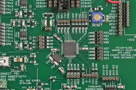
A PCB footprint is the physical layout on a printed circuit board where a component is placed and soldered. It includes the pads (where the component pins connect), silkscreen markings (for identification), and other elements like courtyards (clearance areas). Think of it as the "blueprint" for mounting a component on your board.
Getting the footprint right is critical. A poorly designed footprint can lead to soldering issues, misalignment, or even a non-functional board. For beginners in PCB design, understanding footprints is the foundation of creating reliable circuits. Accurate footprints ensure that components fit perfectly during assembly, prevent short circuits, and meet manufacturing tolerances, saving time and costs.
Key Terms to Know Before Designing PCB Footprints
Before diving into the step-by-step process of creating PCB footprints, let's cover some basic terms to make the tutorial easier to follow:
- Pads: The metal areas on the PCB where component pins are soldered.
- Silkscreen: The printed text or symbols on the PCB for component identification and orientation.
- Courtyard: The boundary around the component to ensure clearance from other parts.
- Land Pattern: Another term for footprint, referring to the arrangement of pads and other elements.
- Pin 1 Indicator: A mark (often a dot or line) showing the orientation of the component.
Understanding these terms will help you navigate design tools and datasheets as you create your first footprint.
Tools You Need for PCB Footprint Design
To start designing PCB footprints, you'll need a design software with a footprint editor. Many popular tools offer free or affordable versions for beginners. These tools allow you to draw pads, set dimensions, and save footprints for reuse. Some widely used options include software with built-in libraries and editors tailored for PCB design.
Most of these tools come with libraries of pre-made footprints, but learning to create custom ones is essential for unique components or specific project needs. Make sure to choose a tool that supports exporting files in formats like Gerber, which are used for manufacturing.
Step-by-Step Guide to Creating PCB Footprints
Now, let's walk through the process of designing a PCB footprint. This easy PCB footprint guide is tailored for beginners, breaking down each step into manageable parts.
Step 1: Gather Component Information
Start by collecting the datasheet for the component you’re designing a footprint for. The datasheet provides critical details like pin spacing, pad sizes, and package dimensions. For example, if you're working on a simple resistor with a 1206 package, the datasheet might specify a length of 3.2 mm, a width of 1.6 mm, and a pad spacing of 2.2 mm.
Pay attention to tolerances as well. Some components may have slight variations in dimensions, so design with a small margin (e.g., 0.1 mm extra on pad sizes) to accommodate manufacturing differences.
Step 2: Set Up Your Design Environment
Open your chosen design software and create a new footprint file. Set the grid to a fine resolution, like 0.1 mm, to allow precise placement of pads and lines. Ensure the units (millimeters or inches) match the datasheet specifications to avoid scaling errors.
Step 3: Draw the Pads
Using the datasheet, place the pads where the component pins will connect. For a through-hole component, use circular or oval pads. For surface-mount devices (SMD), rectangular pads are common. Set the pad dimensions slightly larger than the pin size to ensure good solderability. For instance, if a pin is 0.5 mm wide, a pad width of 0.7 mm provides a safe margin.
Number the pads according to the pin numbers in the datasheet. This helps during schematic linking later on.
Step 4: Add the Silkscreen Layer
The silkscreen layer includes markings to identify the component and its orientation. Draw a simple outline of the component package and add a reference designator (like "R1" for a resistor). Include a dot or line near pin 1 to show the correct orientation. Keep the silkscreen clear of pads to avoid interference during soldering.
Step 5: Define the Courtyard
The courtyard is the clearance area around the component. It prevents overlap with nearby parts during assembly. Typically, add a margin of 0.5 mm to 1 mm beyond the component’s edges, depending on the manufacturing guidelines. Draw a rectangular or custom shape around the footprint to mark this boundary.
Step 6: Verify Against Standards
Check your footprint against industry standards like IPC-7351, which provides guidelines for pad sizes and spacing. Many design tools have built-in calculators or wizards to align your footprint with these standards. For example, IPC-7351 recommends specific pad dimensions for SMD components to ensure reliable soldering.
Step 7: Save and Test Your Footprint
Save the footprint in your library with a clear name, such as "RES_1206" for a 1206 resistor. Then, test it by placing it on a sample PCB layout. Check for alignment issues, clearance violations, or missing elements. If possible, generate a 3D view to visualize how the component fits on the board.
Common Mistakes to Avoid in PCB Footprint Design
As a beginner in PCB design, it’s easy to make errors when creating footprints. Here are some common pitfalls and how to avoid them:
- Incorrect Pad Sizes: Pads that are too small can cause poor soldering, while oversized pads may lead to shorts. Always refer to the datasheet and add a small margin (e.g., 0.2 mm).
- Misaligned Pin Numbers: Ensure pad numbers match the component’s pinout in the datasheet to avoid wiring errors.
- Insufficient Clearance: A courtyard that's too tight can cause components to interfere during assembly. Follow manufacturer spacing rules, often around 0.8 mm minimum.
- Ignoring Thermal Pads: For components like power ICs, include thermal pads if specified in the datasheet to manage heat dissipation.
Tips for Improving Your PCB Footprint Design Skills
Designing footprints gets easier with practice. Here are some tips to help you improve over time:
- Use Existing Libraries: Start with pre-made footprints from your software’s library to understand standard designs before creating custom ones.
- Double-Check Datasheets: Always verify dimensions and tolerances. A small error, like a 0.1 mm mismatch, can ruin a board.
- Learn from Feedback: After manufacturing, review any assembly issues to refine your footprint designs for future projects.
- Stay Updated on Standards: Familiarize yourself with updates to standards like IPC-7351 to keep your designs compatible with modern manufacturing processes.
Why Accurate PCB Footprints Matter for Manufacturing
Accurate PCB footprints are not just about design—they directly impact manufacturing success. During assembly, automated machines rely on precise footprints to place and solder components. A mismatch as small as 0.05 mm can lead to misplaced parts or failed solder joints, increasing production costs by up to 20% due to rework or scrap.
Moreover, footprints affect signal integrity in high-speed designs. For example, improper pad spacing in a 5 GHz RF circuit can cause impedance mismatches, leading to signal loss. By investing time in creating accurate footprints, you ensure a smoother transition from design to finished product.
Resources for Learning More About PCB Footprint Design
If you're eager to dive deeper into beginner PCB design, plenty of resources can help. Look for online tutorials, forums, and guides that cover footprint creation and PCB layout basics. Many design software providers also offer free training videos or documentation to help you master their tools.
Additionally, datasheets and manufacturer application notes often include recommended land patterns for specific components. Use these as starting points to build your skills in creating PCB footprints.
Conclusion: Start Designing PCB Footprints with Confidence
Mastering PCB footprint design is a crucial skill for anyone entering the world of PCB design. By following this step-by-step PCB footprint design tutorial, you've learned the essentials of creating accurate and reliable footprints. From gathering component data to verifying your design against standards, each step builds a foundation for successful projects.
Remember, precision is key. Even small errors can lead to big problems during manufacturing, so take your time to double-check dimensions and clearances. With practice, you'll gain confidence in designing footprints that meet both your project needs and industry requirements. Start small, test often, and soon you'll be creating PCB footprints like a pro!
 ALLPCB


