In the fast-paced world of electronics, designing a high-speed PCB (Printed Circuit Board) is no small feat. Engineers face challenges like maintaining signal integrity (SI) and ensuring EMC (Electromagnetic Compatibility) compliance. So, how do you master high-speed PCB layout? It comes down to using proven techniques such as controlled impedance routing, minimizing crosstalk, and applying advanced grounding strategies. In this detailed guide, we’ll walk you through actionable methods to achieve top-notch performance in your designs, focusing on high-speed PCB design signal integrity, EMC compliance PCB layout, and more.
Why High-Speed PCB Design Matters
As electronic devices become faster and more compact, high-speed PCB design has become critical. Whether it’s for data centers, automotive systems, or consumer gadgets, signals moving at gigabit speeds demand precision. Poor design can lead to signal degradation, interference, or even complete system failure. By focusing on high-speed PCB design signal integrity and EMC compliance PCB layout, you can avoid costly redesigns and ensure reliable performance.
In this blog, we’ll cover the core principles and techniques to help you create boards that handle high-speed signals with ease. Let’s dive into the essentials.
Understanding Signal Integrity in High-Speed PCB Design
Signal integrity refers to the quality of an electrical signal as it travels through a PCB. At high speeds, signals can distort due to reflections, crosstalk, or impedance mismatches. Maintaining high-speed PCB design signal integrity is vital for ensuring data is transmitted without errors.
Here are some key factors that affect signal integrity:
- Reflections: Caused by impedance mismatches, reflections can distort signals. For instance, a signal traveling at 2.5 GHz can experience significant reflection if the trace impedance deviates from the standard 50 ohms.
- Crosstalk: This occurs when signals on adjacent traces interfere with each other, especially at high frequencies.
- Signal Loss: High-frequency signals can lose strength due to dielectric losses in the PCB material or long trace lengths.
To tackle these issues, designers must use specific layout techniques and tools. Let’s explore how to address them effectively.
Key Techniques for High-Speed PCB Design Signal Integrity
1. Controlled Impedance Routing Techniques
One of the cornerstones of maintaining signal integrity is using controlled impedance routing techniques. Impedance control ensures that the trace impedance matches the source and load, minimizing reflections. For high-speed signals like USB 3.0 or PCIe, a typical target impedance is 50 ohms for single-ended signals or 100 ohms for differential pairs.
To achieve this:
- Use PCB design software to calculate trace width and spacing based on the dielectric constant of your board material (often around 4.2 for FR-4).
- Maintain consistent trace geometry by avoiding sharp bends. Use 45-degree angles or curves for turns.
- Route critical traces over a continuous ground plane to provide a stable return path.
By adhering to these practices, you can reduce signal reflections and ensure clean data transmission.
2. Minimizing Crosstalk in PCB Layouts
Crosstalk is a major challenge in high-speed designs, especially when traces are close together. Minimizing crosstalk in PCB layouts requires careful planning of trace spacing and routing.
Follow these tips:
- Increase spacing between high-speed traces. A common rule is the "3W rule," where the spacing between traces is at least three times the width of the trace.
- Route high-speed signals on different layers if possible, separated by ground planes to act as shields.
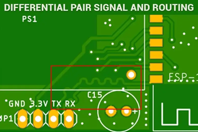
- Use differential signaling for critical paths, as it inherently reduces noise and crosstalk.
Implementing these strategies can significantly lower interference and improve overall performance.
Ensuring EMC Compliance in PCB Layout
Electromagnetic Compatibility (EMC) ensures that your PCB doesn’t emit excessive electromagnetic interference (EMI) and can withstand external interference. Achieving EMC compliance PCB layout is not just about meeting regulatory standards—it’s also about ensuring your device operates reliably in real-world conditions.
High-speed signals are prone to generating EMI due to rapid switching and high frequencies. Without proper design, this interference can disrupt nearby components or other devices. Let’s look at practical ways to design for EMC.
1. Proper Layer Stackup for EMI Control
A well-designed layer stackup is critical for EMC. For high-speed designs, a typical 4-layer stackup might include:
- Top Layer: Signal traces
- Layer 2: Ground plane
- Layer 3: Power plane
- Bottom Layer: Signal traces
The ground and power planes act as shields, reducing EMI by providing low-impedance return paths for high-speed signals. Ensure that high-speed traces are routed adjacent to a ground plane to minimize loop areas that can radiate interference.
2. Filtering and Decoupling for Noise Reduction
Power supply noise can couple into high-speed signals, causing EMI. Place decoupling capacitors close to power pins of ICs to filter out noise. For example, a 0.1 μF capacitor can handle high-frequency noise, while a larger 10 μF capacitor addresses lower-frequency fluctuations.
Additionally, consider using ferrite beads in series with power lines to block high-frequency noise while allowing DC current to pass.
Advanced PCB Grounding Strategies for SI and EMC
Grounding is the backbone of any high-speed PCB design. Poor grounding can lead to signal integrity issues and EMI problems. Using advanced PCB grounding strategies can make a significant difference in performance.
1. Use a Solid Ground Plane
A continuous ground plane provides a low-impedance return path for signals, reducing noise and EMI. Avoid splitting the ground plane unless absolutely necessary, as splits can create high-impedance paths and increase interference.
For multi-layer boards, dedicate an entire layer to ground and ensure it’s unbroken beneath high-speed traces. This minimizes the loop area and keeps return currents close to the signal path.
2. Separate Analog and Digital Grounds
In mixed-signal designs, separate analog and digital ground planes to prevent digital noise from affecting sensitive analog circuits. Connect the two grounds at a single point, often near the power supply, to avoid ground loops.
3. Strategic Via Placement
When routing high-speed signals between layers, place vias carefully. Use ground vias near signal vias to provide a return path and reduce EMI. For example, in a design with 10 GHz signals, placing ground vias within 0.5 mm of signal vias can significantly lower interference.
Thermal Management in High-Speed PCB Design
High-speed circuits often generate significant heat due to high current densities and fast switching. Poor thermal management can degrade signal integrity and shorten component lifespan. Here’s how to address it:
- Use thermal vias to transfer heat from hot components to a ground plane or heat sink.
- Choose PCB materials with better thermal conductivity for high-power designs. For instance, materials with a thermal conductivity of 1 W/mK or higher can help dissipate heat effectively.
- Place heat-generating components away from sensitive high-speed traces to avoid thermal interference.
Tools and Simulations for High-Speed PCB Design
Designing for signal integrity and EMC is complex, but modern tools can simplify the process. Use simulation software to analyze signal behavior before fabrication. Tools can model impedance, crosstalk, and EMI, helping you identify issues early.
- Run pre-layout simulations to optimize trace widths and stackup.
- Perform post-layout analysis to verify signal integrity and EMC performance.
Investing time in simulations can save significant costs by reducing the need for multiple prototypes.
Best Practices for High-Speed PCB Layout
To wrap up, here are some overarching best practices for mastering high-speed PCB layout:
- Keep high-speed traces as short as possible to minimize signal loss.
- Avoid routing high-speed signals near board edges, where EMI can radiate more easily.
- Test your design under real-world conditions to ensure it meets performance and compliance standards.
Conclusion: Elevate Your High-Speed PCB Designs
Mastering high-speed PCB layout is a blend of science and art. By focusing on high-speed PCB design signal integrity, EMC compliance PCB layout, controlled impedance routing techniques, minimizing crosstalk in PCB, and advanced PCB grounding strategies, you can create boards that perform reliably at high speeds. Whether you’re designing for telecommunications, automotive, or consumer electronics, these techniques will help you stay ahead of challenges and deliver top-quality results.
Start applying these methods in your next project to see the difference. With careful planning and the right tools, you can achieve exceptional signal integrity and EMC performance, ensuring your designs stand out in a competitive field.
 ALLPCB


