 ALLPCB


If you're a PCB designer looking to master BGA breakout, you're in the right place. BGA breakout—routing signals from the densely packed pins of a Ball Grid Array (BGA) component to other parts of your printed circuit board—can be a daunting task. But with the right techniques, it becomes manageable. In this guide, we'll cover a BGA breakout tutorial, walk you through a BGA breakout step by step, and share BGA breakout best practices to help you design high-performance, reliable boards.
Whether you're working on high-speed applications or compact designs, this comprehensive resource will provide actionable insights and practical tips to tackle the challenges of BGA routing. Let’s dive into the details and demystify the process.
What Is BGA Breakout and Why Is It Important?
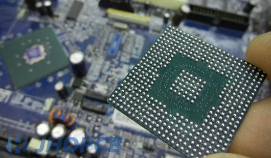
BGA, or Ball Grid Array, is a packaging technology used for integrated circuits, especially in microprocessors, FPGAs, and other high-pin-count components. Unlike traditional packages with pins on the sides, BGA components have an array of solder balls on the underside, allowing for higher density and better performance in smaller spaces. However, this density creates a challenge: routing signals from these tightly spaced balls to the rest of the PCB without interference or errors.
BGA breakout is the process of designing traces and vias to connect these solder balls to other components or layers of the board. Done poorly, it can lead to signal integrity issues, crosstalk, or manufacturing defects. Done well, it ensures reliable performance, even in high-speed or high-density designs. As modern electronics demand more functionality in smaller packages, mastering BGA breakout is essential for any PCB designer.
Key Challenges in BGA Breakout
Before we explore the solutions, it’s important to understand the hurdles you’ll face during BGA breakout. These challenges often stem from the unique nature of BGA packages:
- High Pin Density: BGAs can have hundreds or thousands of pins in a small area, leaving little room for traces.
- Signal Integrity Issues: High-speed signals (often exceeding 1 GHz) are prone to distortion, noise, and crosstalk if not routed carefully.
- Thermal Management: BGAs generate significant heat, and poor design can lead to overheating or uneven thermal distribution.
- Manufacturing Constraints: Small pad sizes and tight spacing require precision in fabrication and assembly, increasing the risk of defects.
Addressing these challenges requires a strategic approach, which we’ll cover in the following sections with a detailed BGA breakout step by step guide.
BGA Breakout Step by Step: A Practical Tutorial
Let’s walk through the process of BGA breakout with a clear, actionable tutorial. Follow these steps to ensure a successful design while maintaining signal integrity and manufacturability.
Step 1: Understand Your BGA Package and Requirements
Start by reviewing the datasheet of your BGA component. Note the pin count, pitch (distance between solder balls, often 0.4mm to 1.0mm), and any specific routing or power requirements. Identify critical signals, such as high-speed differential pairs or power pins, that need priority in routing.
For example, a BGA with a 0.5mm pitch might require microvias for breakout, while a 1.0mm pitch might allow for standard vias. Knowing these details upfront helps you plan your stack-up and routing strategy.
Step 2: Plan Your PCB Stack-Up
A well-designed stack-up is the foundation of successful BGA breakout. Aim for a multilayer board (6 layers or more for complex designs) to provide enough space for signal, power, and ground planes. Dedicate layers to ground and power to minimize noise and ensure stable voltage delivery.
For high-speed designs, consider a stack-up with closely spaced signal and ground layers to control impedance. A common target impedance for high-speed signals is 50 ohms for single-ended traces and 100 ohms for differential pairs.
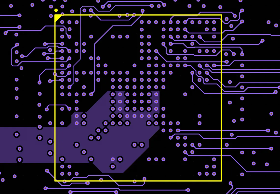
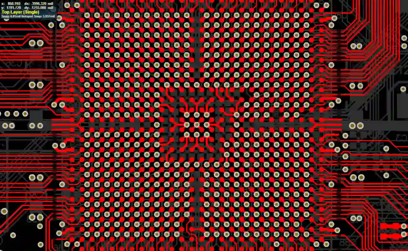
Step 3: Design the BGA Fanout Pattern
Fanout refers to the initial routing of traces from the BGA pads to vias, which then connect to other layers. The goal is to escape the dense grid of pins efficiently. There are two common fanout patterns:
- Dog-Bone Fanout: Used for larger pitch BGAs (0.8mm and above). Traces connect each pad to a via with a short stub, resembling a dog bone shape.
- Via-in-Pad: Used for finer pitch BGAs (0.5mm or less). Vias are placed directly under the pads, saving space but requiring advanced manufacturing techniques like filled vias.
Focus on routing high-priority signals (like clock lines or differential pairs) from the inner pins first, as they are harder to access. Route outer pins last, as they have more space for traces.
Step 4: Route Critical Signals with Care
High-speed signals require special attention to maintain signal integrity. Keep trace lengths short to minimize delay and match lengths for differential pairs to within 5-10 mils (0.127-0.254mm) to avoid skew. Avoid sharp bends; use 45-degree angles or smooth curves to reduce signal reflection.
Place ground vias near signal vias to provide a return path and reduce electromagnetic interference (EMI). Maintain a consistent trace width to achieve target impedance, such as 4-6 mils for 50-ohm traces on standard FR-4 material.
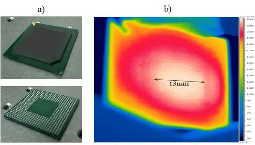
Step 5: Implement Thermal Management
BGAs often run hot, so thermal design is critical. Use thermal vias under the BGA to transfer heat to inner or bottom layers. A grid of 0.3mm vias with 1.2mm spacing can effectively dissipate heat, though this depends on your board’s thickness and material.
Ensure the thermal pad (if present) connects to a large copper plane for heat spreading. Avoid routing signals through this area to prevent interference with thermal performance.
Step 6: Verify Design Rules and Simulate
Run a Design Rule Check (DRC) in your PCB design software to ensure spacing, trace width, and via placement meet manufacturing capabilities. For high-speed designs, use simulation tools to check signal integrity, looking for issues like overshoot or ringing in waveforms.
For instance, a simulation might reveal that a 500 MHz signal experiences crosstalk if traces are spaced less than 10 mils apart. Adjust your layout accordingly to fix such issues before fabrication.
BGA Breakout Best Practices for Optimal Results
Beyond the step-by-step process, adopting these BGA breakout best practices will elevate your design quality and reliability. These tips are based on industry standards and proven techniques.
1. Prioritize Ground and Power Planes
Dedicate entire layers to ground and power to create a low-impedance path for current. This reduces noise and stabilizes voltage, especially for BGAs with high current demands. Place decoupling capacitors (e.g., 0.1μF and 1μF) close to power pins, within 100 mils, to filter out transients.
2. Minimize Via Usage for High-Speed Signals
Each via introduces inductance and capacitance, which can distort high-speed signals above 1 GHz. Use blind or buried vias for inner layer routing to keep signal paths short and clean. If standard vias are unavoidable, keep them to a minimum and ensure a nearby ground via for return current.
3. Optimize Trace Spacing for Signal Integrity
To prevent crosstalk, maintain a spacing of at least 3 times the trace width between adjacent high-speed traces. For a 5-mil trace, this means a 15-mil separation. If space is tight, use ground shielding by placing grounded traces or vias between critical signals.
4. Collaborate with Your Manufacturer Early
BGA designs often push the limits of fabrication technology, especially with fine-pitch components. Share your design files with your PCB manufacturer during the planning stage to confirm capabilities like minimum via size (often 0.2mm) or trace width (down to 3 mils for advanced processes). This prevents costly redesigns later.
5. Test and Iterate Your Design
After fabrication, test your board for signal integrity and thermal performance. Use tools like oscilloscopes to measure signal quality and thermal cameras to identify hot spots. If issues arise, analyze the root cause—such as a mismatched impedance of 60 ohms instead of the target 50 ohms—and adjust your design for the next iteration.
Common Mistakes to Avoid in BGA Breakout
Even experienced designers can make errors when routing BGAs. Here are some pitfalls to watch out for:
- Ignoring Signal Priority: Failing to route critical signals first can leave them trapped behind less important traces, forcing long detours that degrade performance.
- Overloading Layers: Trying to route too many signals on a single layer creates congestion and increases crosstalk risk.
- Poor Thermal Via Placement: Inadequate or unevenly spaced thermal vias can lead to localized overheating, risking component failure.
- Neglecting Manufacturability: Designing without considering fabrication limits, like minimum drill sizes, can result in boards that can’t be built as intended.
By keeping these mistakes in mind, you can proactively design a more robust and reliable PCB.
Tools and Resources for BGA Breakout Success
Modern PCB design software offers features tailored for BGA routing, such as automated fanout tools and impedance calculators. These can save time and reduce errors, especially for complex designs with 500+ pins. Additionally, online resources like application notes from semiconductor manufacturers often provide specific BGA layout guidelines.
Consider joining online forums or communities for PCB designers to exchange tips and solutions for tricky breakout challenges. Staying updated with industry standards, such as those from IPC (Institute of Printed Circuits), can also guide your design decisions.
Conclusion: Mastering BGA Breakout for Better Designs
BGA breakout doesn’t have to be intimidating. By following this BGA breakout tutorial, using the detailed BGA breakout step by step process, and applying BGA breakout best practices, you can confidently tackle even the most complex designs. From planning your stack-up to routing critical signals and ensuring thermal management, each step builds toward a reliable, high-performance PCB.
As electronics continue to shrink and speeds increase, mastering BGA routing will remain a valuable skill for any designer. With careful planning, attention to detail, and collaboration with your manufacturing partner, you’ll create boards that meet the demands of modern technology. Start applying these strategies in your next project, and watch your design quality soar.


