ALLPCB


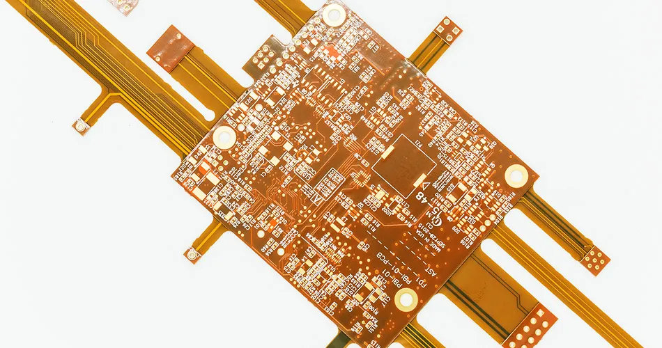
Flexible printed circuit boards enable compact, lightweight electronic designs in applications ranging from wearable devices to automotive sensors. Proper pad-to-pad spacing forms a critical element of flexible PCB design because it directly influences mechanical reliability during bending and flexing. Engineers must account for material properties, bend radius requirements, and stress distribution to prevent failures such as pad cracking or delamination. Inadequate spacing often leads to concentrated bending stress that compromises long-term performance in both static and dynamic flexing PCB environments. Understanding these factors helps designers create robust layouts that meet functional and durability goals.
Why Pad Spacing Matters in Flex PCB Applications
Pad spacing in flex circuits differs from rigid board practices due to the inherent flexibility of the substrate materials. Tight spacing can restrict the ability of traces and pads to move independently during bending, increasing the risk of localized stress concentrations. This becomes especially relevant in dynamic flexing PCB designs where repeated movement occurs over the product lifetime. Industry standards such as IPC-2223 provide design guidelines that address these mechanical considerations for flexible constructions. Proper spacing also supports reliable adhesive bonding and coverlay application, which further protect against environmental and mechanical degradation.
Technical Principles Behind Bending Stress and Pad Design
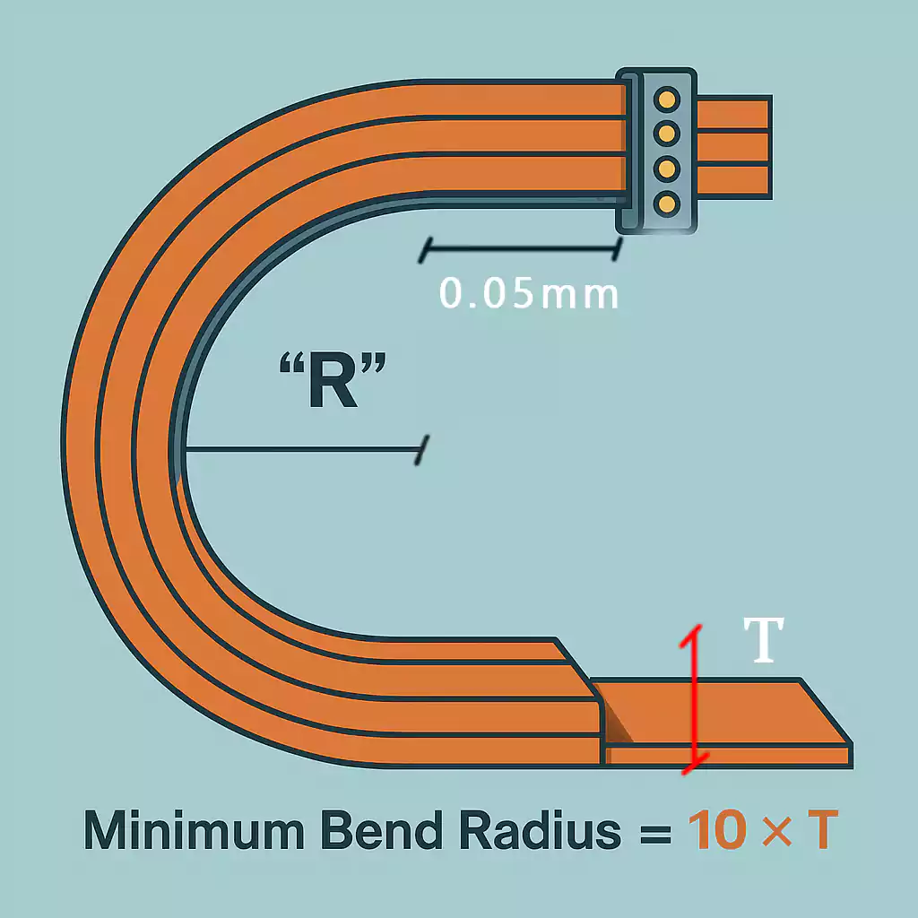
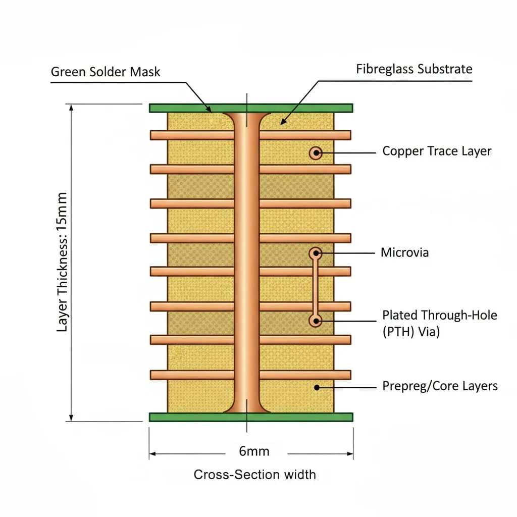
Bending introduces tensile and compressive forces that act differently on copper features depending on their position relative to the neutral axis. When pads sit too close together, the copper cannot deform uniformly, leading to higher shear stresses at the pad edges and interfaces with the dielectric. Adhesive layers between copper and substrate play a key role here because their thickness and modulus influence how stress transfers during flexure. In areas subject to dynamic flexing, even small reductions in pad-to-pad spacing can accelerate fatigue cracking after thousands of cycles. IPC-6013 outlines performance expectations for flexible boards under such mechanical loads, emphasizing the need for adequate feature separation to maintain integrity.
Designers evaluate strain distribution using established bend radius formulas that scale with overall stack-up thickness. Pads placed near bend lines experience amplified effects if spacing does not allow sufficient relief. Coverlay openings must also align properly with pads to avoid additional stress risers from adhesive squeeze-out or misalignment. These mechanisms explain why generic rigid-board spacing rules often prove insufficient for flex applications and why dedicated flexible PCB design rules incorporate mechanical factors alongside electrical ones.
Practical Solutions and Best Practices for Pad Spacing
Begin layout by establishing minimum pad-to-pad spacing based on copper weight, dielectric thickness, and intended bend type. A common starting point involves increasing spacing by 50 to 100 percent compared with rigid equivalents in dynamic zones to accommodate material movement. Staggering pads in a zigzag pattern along bend areas distributes stress more evenly and reduces the chance of simultaneous cracking across multiple features.
Engineers should also maintain adequate clearance between pads and the bend centerline, typically ensuring at least one pad diameter of separation where possible. Adhesive considerations in flex PCB designs require careful selection of low-modulus adhesives that absorb rather than transmit bending forces. Applying these practices consistently helps achieve reliable performance while complying with IPC-2223 recommendations for feature placement.
Additional steps include specifying appropriate coverlay materials and registration tolerances so that openings do not create unintended stress points. Simulation tools can model strain fields early in the design cycle, allowing iterative adjustments before prototyping. Prototypes should undergo bend testing that replicates expected use conditions, including both installation flexing and operational dynamic movement. Documentation of these tests supports traceability and continuous improvement in subsequent designs.
Troubleshooting Common Pad Spacing Issues in Flex Designs
When pad cracking appears after initial flex testing, the first diagnostic step involves measuring actual spacing against design intent and verifying that bend radii meet minimum requirements. Insufficient spacing near transition zones between rigid and flex sections frequently contributes to early failures. Reviewing adhesive thickness and cure conditions can reveal whether bonding layers are contributing excess rigidity.
In cases of intermittent electrical opens, cross-section analysis often shows micro-cracks originating at pad edges where spacing proved marginal. Adjusting layout to increase separation or incorporating strain-relief features such as teardrop pads or additional anchor points resolves many of these issues. Iterative testing with incremental spacing changes provides data to refine rules for future projects.
Conclusion
Effective management of pad-to-pad spacing addresses the distinctive mechanical demands of flexible PCB design. By applying principles from IPC-2223 and IPC-6013, designers can mitigate bending stress while preserving electrical performance. Attention to adhesive selection, coverlay integration, and layout techniques such as staggering further enhances reliability in both static and dynamic applications. Consistent adherence to these practices reduces field failures and supports the growing use of flex circuits across demanding industries.
FAQs
Q1: What minimum pad spacing should be used in flexible PCB design for dynamic applications?
A1: Dynamic flexing PCB layouts typically require greater pad-to-pad spacing than rigid boards to accommodate repeated bending without inducing excessive stress. Guidelines derived from IPC-2223 suggest evaluating spacing based on copper thickness, overall stack-up, and bend radius. Increasing separation by 50 percent or more in flex zones often provides adequate margin while maintaining manufacturability.
Q2: How does bending stress affect pad design in flex PCBs?
A2: Bending stress concentrates at pad edges when spacing is insufficient, leading to potential cracking or delamination over time. Proper pad spacing allows copper features to flex more independently, reducing peak strains. Incorporating design features such as staggered arrangements or increased clearance from bend lines helps distribute forces evenly across the circuit.
Q3: Why are adhesive considerations important for pad spacing in flex PCBs?
A3: Adhesives influence how mechanical loads transfer between copper and substrate during flexing. Stiffer adhesives can amplify stress at closely spaced pads, whereas lower-modulus options provide compliance. Selecting and applying adhesives according to IPC-6013 performance criteria supports long-term pad integrity alongside appropriate spacing rules.
Q4: What layout techniques improve reliability when pad spacing is constrained in flex circuits?
A4: Staggering pads, adding strain-relief fillets, and maintaining extra clearance from bend areas help compensate for tighter spacing. These approaches reduce simultaneous stress on adjacent features and improve fatigue resistance. Early simulation combined with prototype bend testing validates the effectiveness of such modifications before production.