ALLPCB


Why DFM Matters for High-Frequency PCBs
High-frequency printed circuit boards operate at radio frequencies and high data rates where signal integrity becomes critical to overall system performance. Design for manufacturability, or DFM, integrates manufacturing considerations directly into the layout process to reduce defects, improve yield, and maintain electrical performance. Engineers working on RF and high-speed designs must balance electrical requirements with fabrication realities from the earliest stages. Effective DFM practices help avoid costly respins while ensuring boards meet both functional and production standards.
High-frequency circuits are especially sensitive to small variations in trace geometry, material properties, and assembly processes. Even minor deviations can cause impedance mismatches, increased insertion loss, or electromagnetic interference that degrades system reliability. Applying DFM guidelines for RF PCBs early helps align design intent with actual manufacturing capabilities. This approach supports consistent production of boards used in telecommunications, radar, and high-speed digital systems. Without structured DFM, projects often encounter delays during fabrication or testing.
Key Technical Principles in DFM for High-Speed PCB Designs
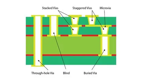
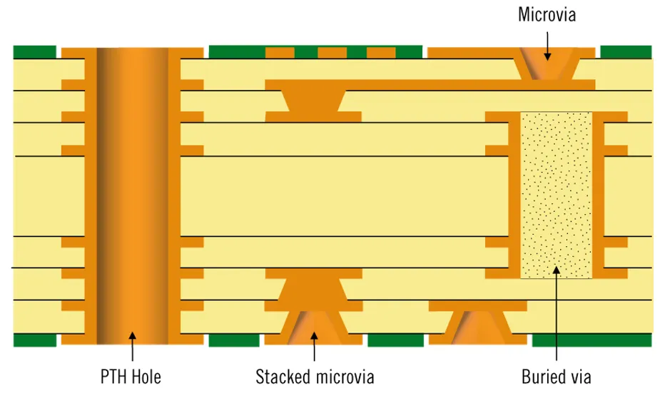
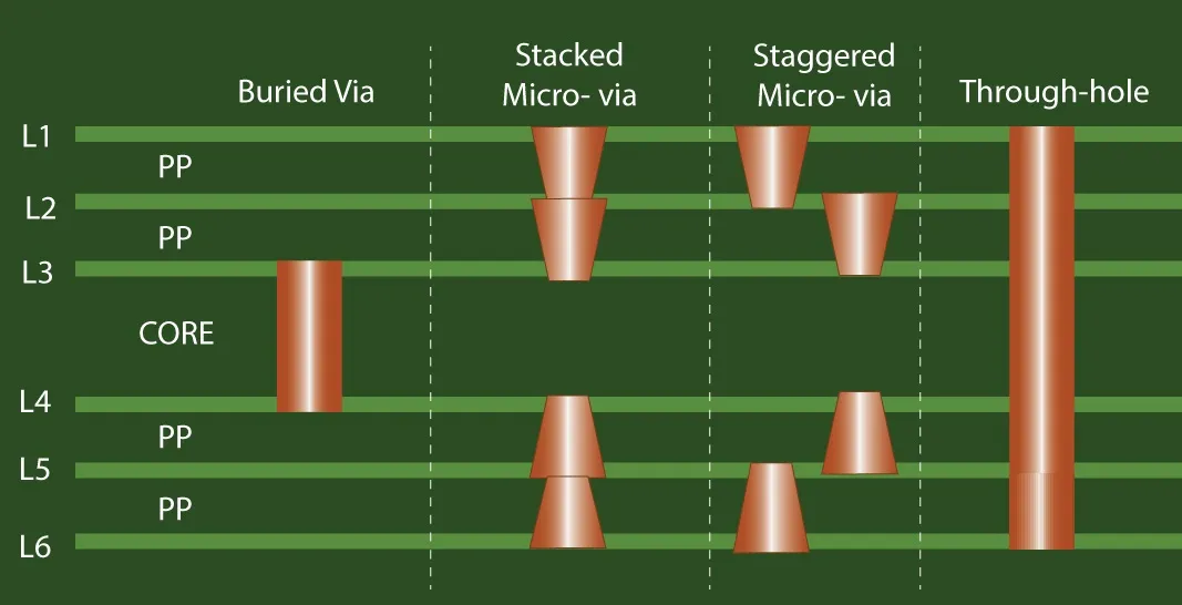
Signal propagation at high frequencies follows principles governed by skin effect and dielectric losses. Conductors carry current primarily on their surfaces, so surface roughness and copper thickness directly influence attenuation. Dielectric materials must exhibit stable dielectric constant and low dissipation factor across the operating frequency range to minimize signal distortion. Via structures introduce inductance and potential discontinuities that require careful modeling and compensation. Thermal expansion differences between layers can also affect long-term reliability in environments with temperature cycling. These mechanisms interact, so designers evaluate them together rather than in isolation.
Manufacturing tolerances become tighter as frequencies increase because wavelength shrinks and features approach the limits of standard processes. Etch factor variations, drill wander, and plating thickness uniformity all influence final electrical behavior. Engineers therefore incorporate margin in trace widths, spacings, and via dimensions during layout. Material selection must also consider moisture absorption and thermal stability to prevent performance drift after assembly. These considerations form the foundation of any DFM checklist high frequency PCB review.
DFM Guidelines and Best Practices for RF PCBs
A practical DFM checklist high frequency PCB begins with stackup definition. Designers specify dielectric thickness, copper weight, and resin content to achieve target impedance while remaining within fabricator capabilities. Controlled impedance calculations should include tolerance analysis that accounts for etch undercut and plating variations. Trace routing avoids sharp bends and maintains consistent reference planes to reduce radiation and crosstalk. Ground vias placed near signal transitions help maintain return path continuity.
Design for manufacturability high speed PCB also addresses panelization and fiducial placement. Proper panel layout maximizes material utilization while providing adequate clearance for routing and testing. Fiducials positioned according to assembly equipment requirements improve placement accuracy during surface-mount processes. Thermal relief patterns around pads prevent excessive heat sinking during soldering yet maintain mechanical strength. Solder mask and silkscreen clearances must prevent bridging on fine-pitch components common in high-speed designs.
Collaboration between design and fabrication teams early in the project identifies potential issues such as minimum feature sizes or aspect ratios that exceed standard capabilities. Documentation should clearly communicate impedance targets, material specifications, and acceptance criteria. This structured exchange reduces ambiguity and supports first-pass success.
Conclusion
Successful high-frequency PCB projects depend on integrating DFM principles throughout the design cycle. Attention to material properties, geometry control, and manufacturing tolerances directly improves both electrical performance and production yield. Engineers who apply these guidelines consistently deliver boards that meet demanding RF and high-speed requirements without unnecessary iterations. The result is reliable hardware delivered on schedule and within budget.
FAQs
Q1: What elements belong on a DFM checklist high frequency PCB?
A1: A typical checklist covers stackup definition, impedance targets with tolerance, trace width and spacing rules, via design parameters, material specifications, and panelization requirements. Each item ties directly to fabrication and assembly capabilities to maintain signal integrity while supporting high yield.
Q2: How do DFM guidelines for RF PCBs differ from standard digital designs?
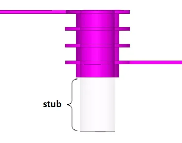
A2: RF and high-frequency guidelines place greater emphasis on dielectric properties, surface roughness, via stub control, and reference plane continuity. These factors become critical because even small variations produce measurable effects on insertion loss and return loss at elevated frequencies.
Q3: Why is design for manufacturability high speed PCB important during stackup planning?
A3: Stackup decisions determine achievable impedance, crosstalk levels, and thermal performance. Early alignment with fabricator capabilities prevents later changes that could shift electrical characteristics or increase cost and lead time.
Q4: What role does material selection play in DFM for high-frequency boards?
A4: Material choice affects dielectric loss, thermal expansion, and moisture sensitivity. Selecting substrates with appropriate electrical and mechanical properties ensures the finished board maintains performance after soldering and throughout its operating life.