ALLPCB


Introduction
High-speed routing in printed circuit boards (PCBs) forms the backbone of modern electronics where data rates exceed gigabits per second. Engineers must prioritize signal integrity and minimize electromagnetic interference to prevent performance degradation in applications such as data centers and automotive systems. Improper routing introduces reflections, crosstalk, and unintended radiation that compromise system reliability. This article delves into structured techniques grounded in engineering principles, offering logical guidance for electric engineers tackling these challenges. By understanding transmission line behavior and layout strategies, designers can achieve robust high-speed designs.

What Is High-Speed Routing and Why It Matters
High-speed routing refers to the placement and shaping of conductive traces on a PCB that carry signals with fast rise times, typically below 100 picoseconds, or frequencies above 1 GHz. At these speeds, traces behave as transmission lines rather than simple wires, demanding controlled impedance and minimal discontinuities. Signal integrity and minimizing electromagnetic interference become critical as mismatches cause ringing, overshoot, and eye diagram closure. Electromagnetic interference arises from radiating currents on traces, potentially violating regulatory limits and causing failures in nearby circuits.
The relevance intensifies with increasing clock speeds in processors and interfaces. Poor routing leads to bit errors, increased power consumption from retransmissions, and costly redesigns. Adhering to guidelines in IPC-2221C ensures designs meet performance expectations across manufacturing variations. Ultimately, mastering high-speed routing directly impacts product success in competitive markets.
Technical Principles of High-Speed Signal Propagation
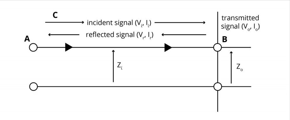
Transmission line theory underpins high-speed routing, where signal voltage waves propagate along traces at speeds determined by the dielectric constant of the PCB material. Characteristic impedance, typically 50 ohms single-ended or 100 ohms differential, must match source and load to avoid reflections quantified by the reflection coefficient formula. Discontinuities like bends, vias, or impedance steps cause partial reflections, distorting waveforms and degrading signal integrity. Crosstalk occurs through capacitive and inductive coupling between adjacent traces, with near-end and far-end effects scaling with trace length and separation.
Electromagnetic interference stems from time-varying currents forming loops that act as antennas, radiating energy proportional to the loop area and frequency squared. Common-mode noise on differential pairs exacerbates this, converting differential signals to radiating modes. Ground bounce from simultaneous switching further couples noise into signals. Standards like IPC-2141A provide models for calculating these effects, emphasizing symmetric routing geometries.
Return paths play a pivotal role, as signals require low-impedance ground or power planes immediately adjacent to traces for image current flow. Splitting planes creates high-inductance paths, amplifying noise. Skin effect confines currents to trace surfaces at high frequencies, increasing effective resistance and losses. These principles dictate that routing must preserve signal integrity and minimize electromagnetic interference through geometry control.
Layer Stackup and Impedance Control
A well-planned layer stackup is foundational, allocating inner layers for signals sandwiched between ground planes in stripline configuration to shield fields and reduce radiation. Microstrip routing on outer layers exposes one side to air, increasing EMI risk, so reserve it for lower speeds. Dielectric thickness and trace width determine impedance via formulas outlined in IPC-2141A, requiring field solvers for precision across frequencies. Manufacturing tolerances necessitate wider margins, typically 10-15 percent variation.
Controlled impedance demands consistent reference planes without splits under traces, ensuring uniform return paths. Power planes should couple tightly to ground via stitching vias to suppress resonances. Hybrid stackups balance signal count with isolation, prioritizing high-speed nets on dedicated layers.
Routing Strategies for Single-Ended Signals
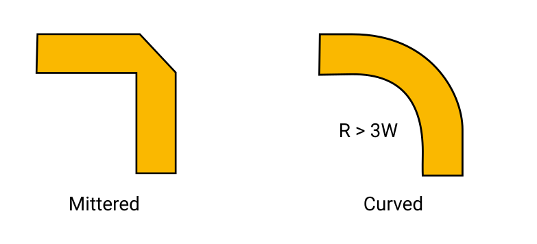
For single-ended signals, minimize trace length to reduce attenuation and delay skew, routing perpendicular to splits in reference planes. Use 135-degree mitered bends instead of 90-degree corners to avoid impedance bumps and reflections from excess copper. Space traces at least 3-5 times width to limit crosstalk below 1 percent of signal amplitude. Avoid routing over clock signals or power supplies to prevent coupling.
Vias introduce stubs that resonate at quarter-wave frequencies, so back-drill or use blind/buried types for critical nets. Minimize via count by fanning out components strategically during placement. These practices directly enhance signal integrity and minimize electromagnetic interference.
Differential Pair Routing Techniques
Differential pairs transmit signals as balanced pairs, rejecting common-mode noise and enabling higher data rates. Maintain constant spacing and length matching within 0.1 mm over the entire length to preserve balance and minimize skew-induced jitter. Route pairs tightly coupled, with edge-coupled geometry on the same layer, and equal width for 100-ohm impedance. Avoid crossing splits or layer changes without symmetric vias.
Intra-pair spacing should be 5-10 times trace width for low crosstalk, while inter-pair separation exceeds 10 times width. Serpentine meanders for length tuning introduce inductance variations, so use smooth trombone patterns. Ground planes beneath pairs contain fields, crucial for EMI suppression.
Advanced Practices: Vias, Length Tuning, and Shielding
Via optimization involves larger antipads and close ground vias to reduce stub length and inductance. For transitions, use via-in-pad or embedded types in high-density boards. Length tuning aligns arrival times, critical for DDR or PCIe interfaces, using dynamic phase adjustments during routing.
Shield traces between sensitive pairs absorb crosstalk, grounded at both ends. Guard rings around clocks contain radiation. Decoupling capacitors near drivers provide clean return currents. IPC-6012F verifies these features endure fabrication stresses like plating variations.
Troubleshooting High-Speed Routing Issues
Engineers often encounter eye closure from excessive jitter, traced to unmatched lengths or poor termination. Measure time-domain reflectometry to identify impedance discontinuities, then adjust widths or add series resistors. Crosstalk manifests as glitches; increase spacing or add shielding. EMI failures in testing reveal loop areas; flood unused spaces with ground pours connected via stitching.
Simulate pre-layout with 3D solvers to predict issues, correlating with hardware measurements. Iterate stackup if resonances persist. Systematic verification per standards resolves most problems efficiently.
Conclusion
High-speed routing techniques revolve around controlled impedance, symmetric geometries, and solid referencing to uphold signal integrity and minimize electromagnetic interference. From stackup planning to via management, each decision builds cumulative performance. Electric engineers benefit from logical adherence to principles in IPC standards, ensuring designs scale reliably. Implementing these practices reduces iterations and accelerates time-to-market.
FAQs
Q1: How does controlled impedance routing improve signal integrity and minimize electromagnetic interference?
A1: Controlled impedance matches trace characteristics to driver and receiver, preventing reflections that distort waveforms. It confines fields tightly between trace and plane, reducing radiation. Per IPC-2141A guidelines, consistent 50-ohm single-ended or 100-ohm differential values across manufacturing tolerances ensure clean propagation. This approach also lowers crosstalk by stabilizing coupling.
Q2: What are the best layer strategies for high-speed signals to preserve signal integrity?
A2: Prioritize stripline inner layers with adjacent ground planes for field containment and low EMI. Avoid outer microstrip for critical nets due to higher radiation. Symmetric stackups per IPC-2221C balance density and performance. Continuous planes without splits under traces provide low-inductance returns.
Q3: Why is length matching essential in differential pair routing for signal integrity?
A3: Length matching within 0.1 mm minimizes skew, preserving differential balance and reducing common-mode conversion. This prevents jitter that closes eye diagrams at high data rates. Proper tuning also aids EMI compliance by avoiding phase misalignment. Engineers verify via timing analysis tools.
Q4: How can vias impact electromagnetic interference in high-speed PCBs?
A4: Vias create stubs acting as resonators, radiating at specific frequencies and coupling noise. Minimize count, use back-drilling, and add ground stitching to shorten stubs and provide returns. IPC-6012F performance specs guide via quality for integrity.
References
IPC-2141A - Design Guide for High-Speed Controlled Impedance Circuit Boards. IPC, 2004
IPC-2221C - Generic Standard on Printed Board Design. IPC, 2023
IPC-6012F - Qualification and Performance Specification for Rigid Printed Boards. IPC, 2023