 ALLPCB


Introduction
PCIe Gen5 represents a significant advancement in high-speed interfaces, operating at data rates that demand precise PCB design to maintain signal integrity. With its doubled bandwidth compared to previous generations, PCIe Gen5 pushes the limits of traditional PCB fabrication and layout techniques. Engineers must address challenges like increased attenuation, reflections, and noise coupling to ensure reliable performance in applications such as data centers, AI accelerators, and high-performance computing. High-speed PCB PCIe Gen5 design requires a holistic approach, integrating material selection, routing strategies, and stackup planning. This article explores the critical considerations for bandwidth optimization and signal integrity in PCIe Gen5 layouts. By following structured engineering principles, designers can achieve robust interfaces capable of sustaining 32 GT/s per lane.
Understanding PCIe Gen5 and Its Demands on PCB Design
PCIe Gen5, or PCI Express 5.0, doubles the data rate of Gen4 to 32 GT/s per lane, enabling unprecedented bandwidth for multi-lane configurations like x16 slots. This interface serves as the backbone for modern servers, GPUs, and storage systems, where aggregate throughput can exceed hundreds of gigabytes per second. The higher frequencies introduce steeper rise times and greater sensitivity to imperfections in the transmission channel, making signal integrity paramount. Without proper high-speed PCB PCIe Gen5 design, issues such as eye closure, jitter accumulation, and bit error rates can degrade performance. Industry relevance stems from the exponential growth in data-intensive workloads, necessitating PCBs that preserve signal quality over longer traces. Engineers targeting electric engineers must prioritize these factors to meet compliance and functionality goals.
The transition to PCIe Gen5 amplifies the need for controlled environments in PCB design. Traditional FR-4 materials often fall short due to higher dielectric losses at these frequencies, prompting a shift toward specialized low-loss dielectrics. Layout complexity increases with requirements for symmetric stackups and minimal via transitions. Bandwidth scaling linearly with lane count underscores the importance of per-lane optimization. Signal integrity directly impacts link training and equalization effectiveness. Thus, PCIe Gen5 layout demands meticulous planning from schematic capture through fabrication.
Fundamental Signal Integrity Principles for PCIe Gen5
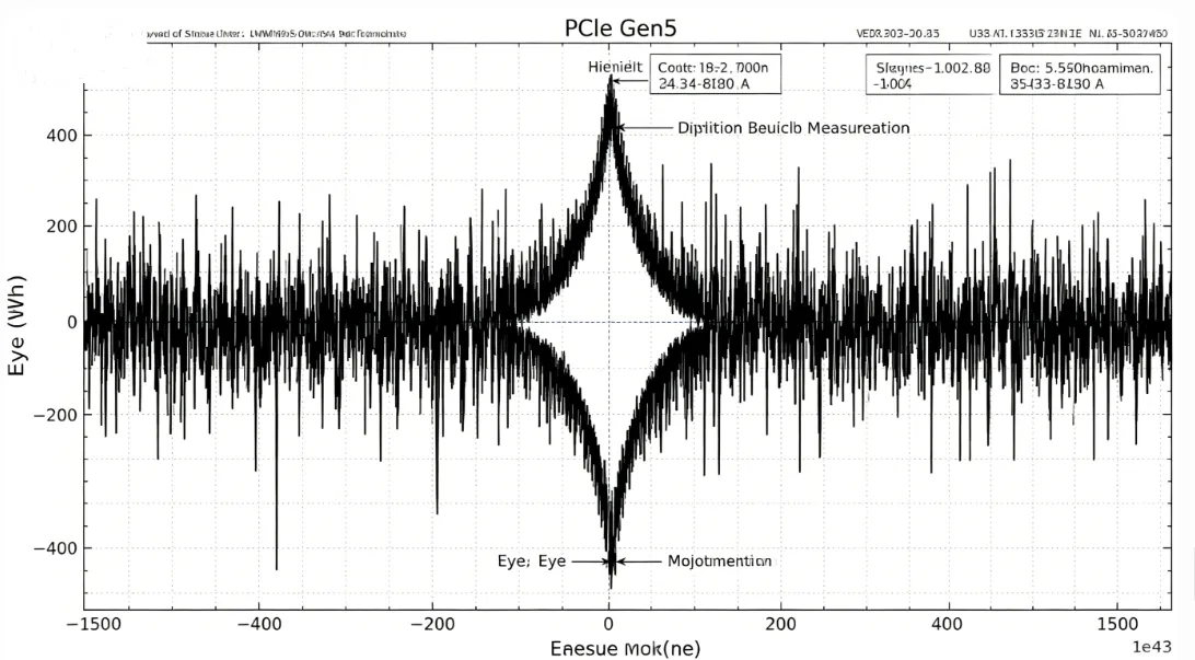
Signal integrity in high-speed PCB PCIe Gen5 design revolves around preserving the electrical characteristics of differential signals throughout the channel. At 32 GT/s, signals experience significant attenuation from conductor losses, dielectric absorption, and skin effect, necessitating low-loss paths. Reflections arise from impedance discontinuities at vias, bends, or transitions, which can cause overshoot and ringing. Jitter, both deterministic and random, accumulates over the link, closing the eye diagram and limiting reach. Crosstalk between adjacent pairs introduces noise that equalizers struggle to correct. Engineers must model these effects using time-domain reflectometry and frequency-domain simulations to predict behavior.
Impedance control forms the cornerstone of signal integrity for differential pairs in PCIe Gen5. Each pair must maintain a consistent characteristic impedance, typically targeted through precise trace width, spacing, and reference plane proximity. Variations due to manufacturing tolerances or glass weave skew can detune the pair, leading to return loss. Per IPC-2221 guidelines, design rules should account for etch factors and copper weight to achieve uniformity. Stackup symmetry ensures balanced fields, minimizing common-mode conversion. Pre-layout verification confirms tolerances within acceptable bounds for Gen5 margins.
Related Reading: Differential Pair Routing: Techniques for High-Speed PCB Layouts
Crosstalk mitigation requires strategic routing geometries in PCIe Gen5 layout. Aggressor-victim coupling increases with proximity and length, far-end crosstalk being particularly detrimental due to its in-phase addition to the victim signal. Minimum spacing rules, often three times the trace width, reduce near-end and far-end effects. Orthogonal routing between layers further suppresses coupling through broadside interactions. Ground planes act as shields, but stitching vias prevent slot resonances. Length staggering of adjacent pairs avoids coherent noise buildup.
Bandwidth Optimization Through PCB Materials and Stackup
Achieving full PCIe Gen5 bandwidth hinges on selecting PCB materials with low dissipation factor and stable dielectric constant. Standard laminates exhibit excessive insertion loss at 16 GHz fundamental and higher harmonics, compressing the receive eye. Low-loss materials reduce dielectric attenuation, extending channel length while maintaining flat frequency response. Glass weave orientation impacts skew in tightly spaced pairs; spread-glass variants minimize this asymmetry. Resin content uniformity prevents Dk gradients that cause intra-pair delay mismatch. Material characterization data guides stackup planning for optimal performance.
Stackup design in high-speed PCB PCIe Gen5 design influences both signal integrity and bandwidth. Symmetric builds with dedicated high-speed signal layers flanked by ground planes provide continuous return paths and field confinement. Core and prepreg thicknesses dictate impedance, requiring iterative field solver adjustments. Thin dielectrics enable tighter coupling for better common-mode rejection. Via optimization, such as backdrilling or blind vias, reduces stub effects that resonate at Gen5 frequencies. Power plane pairing with decoupling supports clean references without impedance drops.
PCIe Gen5 interfaces benefit from hybrid stackups combining low-loss outer layers for signals and cost-effective inners for power. This balances performance and economics while preserving bandwidth. Thermal management integrates with stackup via thicker coppers or embedded planes, preventing hotspots that warp traces. Fabrication processes must align with IPC-6012 performance specifications to ensure material integrity post-lamination. Bandwidth realization depends on this integrated approach.
Related Reading: Unlocking High-Speed Performance: A Deep Dive into 10-Layer PCB Stackup Design
Best Practices for PCIe Gen5 Layout and Routing
Effective PCIe Gen5 layout begins with component placement to minimize trace lengths and layer counts. Connectors and retimers should align with BGA escapes, grouping lanes by direction to simplify routing. Differential pairs demand tight coupling throughout, with intra-pair length matching under 1 mil to preserve polarity. Serpentine meanders equalize total lengths across lanes, avoiding phase skew during training. Avoid 90-degree bends; use 45-degree or curved transitions to reduce reflections.
Routing high-speed PCB PCIe Gen5 design emphasizes layer transitions and via management. Staggered via grids prevent anti-pad resonances, while filled vias maintain plane continuity. Reference planes under signals suppress radiation and EMI. For impedance control, route in stripline over microstrip to shield from external noise. Crosstalk budgets dictate pair-to-pair spacing, with guard traces or ground lines as additional barriers. Post-route extraction verifies S-parameters against link budgets.
Fabrication and assembly considerations enhance signal integrity. Specify low-roughness copper foils to cut conductor losses, paired with spread-glass cores. Test coupons on panels validate impedance and loss profiles. Per IPC-A-600 acceptability criteria, inspect for plating voids or etch undercut that compromise pairs. Controlled impedance boards require fab feedback loops for tolerance. These practices ensure PCIe Gen5 interfaces achieve targeted BER.
Troubleshooting Common PCIe Gen5 Signal Integrity Issues
Engineers often encounter intermittent link failures in PCIe Gen5 prototypes due to subtle SI violations. Excessive insertion loss manifests as training timeouts, resolvable by shortening traces or adding retimers. Jitter peaking from via stubs requires backdrilling verification. Crosstalk hotspots appear in dense areas; widen spacing or reroute orthogonally. Impedance drifts post-reflow stem from CTE mismatches; select compatible materials.
Simulation-discrepancy troubleshooting involves calibrating models with TDR measurements. Fabricator communications clarify process variations like etchback. Field failures trace to thermal expansion skewing pairs; validate with VTDR. Systematic debugging, starting from bathtub curves, isolates root causes. These insights refine future high-speed PCB PCIe Gen5 designs.
Conclusion
High-speed PCB PCIe Gen5 design demands rigorous attention to signal integrity, impedance control, and crosstalk management to unlock its full bandwidth potential. From material selection to precise routing, each decision impacts channel performance at 32 GT/s. Low-loss PCB materials, symmetric stackups, and disciplined layout practices form the foundation for reliable interfaces. Adhering to standards like IPC-2221 and IPC-6012 ensures manufacturability and quality. Engineers equipped with these considerations can deliver robust PCIe Gen5 layouts for demanding applications. Future iterations will build on these principles as data rates escalate.
FAQs
Q1: What are the primary signal integrity challenges in high-speed PCB PCIe Gen5 design?
A1: Signal integrity challenges include high insertion loss, impedance discontinuities, and crosstalk in differential pairs. At 32 GT/s, dielectric and conductor losses compress the eye, while reflections from vias cause jitter. Effective mitigation involves low-loss materials, tight impedance control, and optimized spacing. PCIe Gen5 layout must prioritize symmetric stackups to maintain balance.
Q2: How does impedance control affect PCIe Gen5 interface performance?
A2: Impedance control ensures minimal reflections and maximum power transfer in differential pairs. Variations lead to return loss, degrading signal quality and link margins. Target consistent values through stackup design and fab specs. This practice aligns with IPC-2221 guidelines for high-speed designs, supporting reliable bandwidth.
Q3: Why are low-loss PCB materials essential for PCIe Gen5?
A3: Low-loss materials reduce attenuation at high frequencies, preserving signal amplitude over longer channels. High Df laminates cause excessive dielectric loss, limiting reach. Select options with low Dk skew for uniform propagation. This enables PCIe Gen5 layouts to meet bandwidth without excessive equalization.
Q4: What layout techniques minimize crosstalk in PCIe Gen5 differential pairs?
A4: Minimize crosstalk by enforcing minimum spacing, orthogonal layer routing, and ground shielding. Tightly couple pairs while isolating aggressors. Length staggering prevents coherent interference. These techniques enhance signal integrity in dense high-speed PCB PCIe Gen5 designs.
References
IPC-2221B — Generic Standard on Printed Board Design. IPC, 2009
IPC-6012E — Qualification and Performance Specification for Rigid Printed Boards. IPC, 2017
IPC-A-600K — Acceptability of Printed Boards. IPC, 2020


