 ALLPCB


Introduction
High Density Interconnect (HDI) PCBs represent a cornerstone of modern electronics, enabling compact designs with finer features, microvias, and higher component densities. The choice of substrates in HDI PCB materials directly influences signal integrity, thermal management, and overall reliability in demanding applications like smartphones, automotive systems, and medical devices. Engineers must navigate a complex landscape of material properties to optimize performance while adhering to manufacturing constraints. Poor substrate selection can lead to issues such as signal loss, warpage, or delamination during assembly. This masterclass explores HDI PCB material selection, focusing on critical attributes like glass transition temperature (Tg) and dielectric constant (Dk). By understanding these factors, electric engineers can make informed decisions that balance cost, performance, and manufacturability.
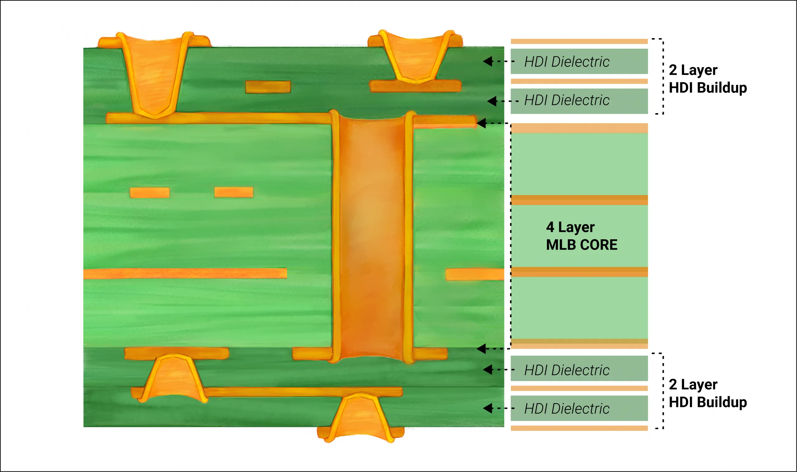
Substrates form the foundational dielectric layers in HDI structures, supporting sequential build-up processes with blind, buried, and stacked vias. Standard FR-4 serves as a baseline, but advanced HDI designs often require enhancements for high-speed signals and thermal cycling. Key considerations include compatibility with laser drilling for microvias and stability under reflow soldering conditions.
What Are HDI PCB Substrates and Why Do They Matter?
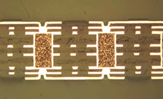
HDI PCB substrates are the insulating core and prepreg materials that provide mechanical support and electrical isolation between conductive layers. In HDI constructions, these materials must accommodate finer pitches, typically below 0.1 mm, and multiple lamination cycles. Unlike standard PCBs, HDI substrates endure additional stresses from via formation and interlayer alignment, making material selection pivotal for yield and longevity.
The relevance stems from the push toward miniaturization and higher operating frequencies in electric engineering projects. Substrates with suboptimal properties can degrade signal quality through increased insertion loss or cause mechanical failures via coefficient of thermal expansion (CTE) mismatches. For instance, in high Tg HDI PCB applications, elevated temperatures during lead-free soldering demand materials that resist softening. According to IPC-2226, design standards for high density interconnects emphasize substrate qualifications to ensure via reliability and planar surfaces.
Furthermore, substrate choice impacts cost efficiency in production scales. Engineers evaluating HDI PCB materials must weigh electrical performance against processability, as laser-drillable resins prevent resin smear during microvia formation. This foundational role underscores why HDI PCB material selection remains a critical engineering decision.
Key Properties of Substrates in HDI PCB Materials
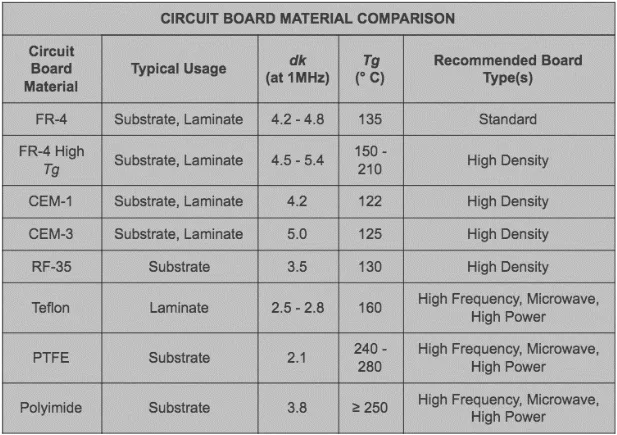
Selecting substrates for HDI PCBs hinges on several interconnected properties that govern electrical, thermal, and mechanical behavior. The glass transition temperature (Tg) marks the point where the material shifts from glassy to rubbery state, affecting dimensional stability above typical soldering thresholds. High Tg HDI PCB materials, often exceeding 170°C, minimize warpage and delamination in multilayer builds subjected to thermal excursions.
Dielectric constant (Dk) and dissipation factor (Df) dominate high-speed performance. Low Dk HDI PCB substrates, ideally below 3.5 at operating frequencies, reduce signal propagation delays and capacitance. Low Df values, typically under 0.005, curb energy loss, preserving waveform integrity in gigabit data rates. These properties become crucial as trace lengths shorten and densities rise in HDI layouts.
Coefficient of thermal expansion (CTE) ensures compatibility with copper foil, preventing cracks during temperature ramps. Z-axis CTE below 70 ppm/°C aligns closely with metal expansion, vital for stacked microvias. Moisture absorption influences dielectric stability, as absorbed water elevates Dk and risks hydrolysis in humid environments.
Thermal conductivity aids heat dissipation in power-dense designs, though it often trades off with low Dk. Laser drillability, characterized by clean ablation without carbon residue, supports aspect ratios up to 1:1 for microvias under 100 μm. IPC-6012E qualification specifications outline performance metrics for these attributes in rigid printed boards, guiding qualification tests.
Technical Principles of HDI PCB Material Performance
The engineering mechanisms behind substrate behavior in HDI PCBs revolve around dielectric polarization and viscoelastic responses. At high frequencies, Dk determines phase velocity via the relation v = c / sqrt(Dk), where lower values accelerate signals and mitigate skew in differential pairs. Df quantifies tan δ, the ratio of lost to stored energy, escalating losses exponentially with frequency due to molecular friction.
Thermal stability links to Tg through polymer chain mobility; below Tg, rigid epoxy networks maintain modulus, but excursions induce creep. High Tg HDI PCB formulations incorporate phenolic or bismaleimide resins for cross-linking density, enhancing resistance to solder reflow peaks around 260°C. CTE mismatches induce via barrel stress, modeled by σ = E * Δα * ΔT, where E is modulus, underscoring low-CTE fillers like silica.
Mechanical integrity during lamination cycles demands low resin flow to avoid interlayer shorts, balanced with sufficient flow for via fill. Laser interaction principles favor UV or CO2 wavelengths that vaporize resin selectively, minimizing heat-affected zones. These principles inform HDI PCB material selection for applications spanning RF modules to computing.
Best Practices for HDI PCB Material Selection
Begin HDI PCB material selection by defining application requirements: operating frequency dictates low Dk/Df priorities, while thermal budgets favor high Tg options. Map signal speeds to loss budgets; for 10 Gbps+, target Dk <3.2 and Df <0.003. Consult datasheets for frequency-dependent curves, as Dk rises with humidity.
Assess build type per IPC-2226; Type II passive builds tolerate standard FR-4, but Type IV active drills demand enhanced drillability. Verify CTE matching across axes, prioritizing Z-axis control for via reliability. Prototype with thermal cycling per IPC-6012E to validate warpage under -40°C to 125°C.
Integrate supplier qualifications early, focusing on UL ratings and RoHS compliance. For low Dk HDI PCB needs, hybrid stacks combine FR-4 cores with low-loss prepregs. Cost-model via fill factors and lamination yields, as advanced resins inflate expenses by 20-50%.
Collaborate across design and fabrication teams to align stackups. Simulate impedance with field solvers incorporating material models. Final validation through signal integrity tests confirms selections.
Common Challenges in HDI Substrates and Mitigation Strategies
Warpage plagues high Tg HDI PCB due to asymmetric CTE, exacerbated in thin cores. Symmetric stackups and carrier foils during buildup counteract this. Via reliability fails from electromigration in high-current densities; low Df reduces thermal hotspots.
Signal skew in low Dk HDI PCB arises from weave-induced anisotropy; spread-glass fabrics homogenize Dk. Moisture-induced CAF (conductive anodic filamentation) requires low absorption resins. JEDEC J-STD-020E moisture sensitivity classifications guide preconditioning.
Conclusion
Mastering HDI PCB materials demands a systematic evaluation of Tg, Dk, Df, CTE, and process compatibility. High Tg HDI PCB ensures thermal robustness, while low Dk variants excel in speed-critical realms. Adhering to standards like IPC-2226 and IPC-6012E fortifies designs against field failures. Electric engineers benefit from iterative prototyping and cross-disciplinary input in HDI PCB material selection. Ultimately, optimal substrates elevate PCB performance, shrinking footprints without compromising reliability.
FAQs
Q1: What makes high Tg HDI PCB materials essential for modern designs?
A1: High Tg HDI PCB materials, with Tg above 170°C, prevent deformation during lead-free reflow and multiple laminations. They maintain mechanical integrity under thermal stress, reducing risks of delamination or via cracking. This property aligns with IPC-2226 guidelines for HDI builds, ensuring reliability in compact electronics. Selection depends on peak exposure temperatures in assembly processes.
Q2: How do low Dk HDI PCB substrates improve signal performance?
A2: Low Dk HDI PCB substrates minimize propagation delays and crosstalk by lowering capacitance per unit length. With Dk values around 3.0-3.5, they support higher data rates beyond 5 Gbps with reduced skew. Low Df complements this by curbing attenuation. Engineers prioritize them for RF and high-speed digital applications during HDI PCB material selection.
Q3: What factors guide HDI PCB material selection for thermal management?
A3: Key factors include Tg for stability, CTE matching to copper, and thermal conductivity for dissipation. Z-axis CTE below 70 ppm/°C prevents warpage in multilayer HDI. High Tg options handle soldering peaks, while simulations predict stress. Balance these with electrical needs per application specs.
Q4: Which standards regulate HDI PCB substrates?
A4: IPC-2226 provides design rules for HDI features, including substrate qualifications. IPC-6012E specifies performance for rigid boards with HDI elements. These ensure via integrity and planar lamination. Compliance verifies material suitability through qualification testing.
References
IPC-2226 - Design Standard for High Density Interconnects. IPC.
IPC-6012E - Qualification and Performance Specification for Rigid Printed Boards. IPC, 2017.
IPC-A-600K - Acceptability of Printed Boards. IPC, 2020.


