 ALLPCB


Introduction
High-frequency circuits form the backbone of modern communication systems, radar equipment, and advanced computing platforms. Engineers encounter high-frequency signal issues when operating frequencies rise above several hundred megahertz. These challenges manifest as unexpected distortions that degrade overall system performance. Proper management of trace impedance becomes essential to maintain reliable data transmission. Designers must address these concerns early in the development cycle to avoid costly revisions.
Why Signal Integrity Matters in High-Frequency Circuits
Signal integrity directly influences the accuracy and speed of electronic devices operating at elevated frequencies. Poor integrity leads to bit errors, reduced range, and increased power consumption. Industry professionals recognize that even minor deviations in circuit behavior can compromise entire systems. Trace impedance control ensures consistent signal paths across the board. Addressing these factors supports compliance with established performance expectations in demanding applications.
Technical Principles Behind High-Frequency Signal Issues
Several physical mechanisms contribute to high-frequency signal issues in printed circuit boards. Signal attenuation occurs as electromagnetic waves lose energy while traveling along conductors. This loss increases proportionally with frequency, shortening the effective transmission distance. Engineers analyze these effects through simulation tools and measurement techniques to predict behavior accurately.
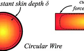
The skin effect plays a prominent role at higher frequencies. Current concentrates near the surface of conductors, reducing the effective cross-sectional area available for flow. Consequently, resistance rises and further contributes to signal attenuation. Designers account for this phenomenon by selecting appropriate conductor thicknesses and materials during layout.
Dielectric loss represents another critical factor. Energy dissipates within the insulating materials surrounding the traces as the electric field alternates rapidly. Materials with higher loss tangents exacerbate this effect, leading to greater overall attenuation. Careful material selection helps minimize these losses while maintaining mechanical stability.
Trace impedance must remain consistent to prevent reflections and ringing. Variations arise from changes in trace width, spacing, or the surrounding dielectric environment. Controlled impedance design practices ensure that signals propagate without distortion. Structured calculations based on geometry and material properties guide these decisions.
Related Reading: Understanding PCB Trace Impedance: Factors, Calculations, and Control Techniques
Practical Solutions and Best Practices
Engineers apply several techniques to mitigate high-frequency signal issues during the design phase. Maintaining uniform trace widths and employing ground planes reduces impedance variations. Differential pair routing further improves noise immunity in critical paths. These approaches help preserve signal quality across the operating bandwidth.
Related Reading: Differential Pair Routing: Techniques for High-Speed PCB Layouts
Material choices significantly influence performance outcomes. Low-loss dielectrics reduce both dielectric loss and overall attenuation. Board stack-up planning ensures consistent impedance values throughout the circuit. Simulation software validates these choices before fabrication begins.
Layout strategies include minimizing via counts and avoiding sharp bends in high-speed traces. Proper termination techniques match source and load impedances to eliminate reflections. Regular design reviews verify compliance with target specifications. These steps collectively enhance reliability in high-frequency environments.
Conclusion
Effective management of high-frequency signal issues requires attention to signal attenuation, skin effect, dielectric loss, and trace impedance from the outset. Structured engineering practices deliver consistent results across diverse applications. Continued adherence to proven methods supports the development of robust electronic systems. Professionals who integrate these principles achieve superior performance and reduced development cycles.
FAQs
Q1: What causes signal attenuation in high-frequency circuits?
A1: Signal attenuation arises primarily from conductor losses and dielectric absorption as frequency increases. The skin effect concentrates current flow and elevates resistance, while dielectric loss dissipates energy in the substrate. Engineers mitigate these effects through material selection and careful trace design to maintain acceptable signal levels.
Q2: How does the skin effect impact trace impedance?
A2: The skin effect reduces the effective conductor area at higher frequencies, increasing resistance and altering characteristic impedance. This change can lead to mismatches if not accounted for during layout. Consistent trace geometry and appropriate material thickness help stabilize impedance values across the frequency range.
Q3: Why is dielectric loss important for high-frequency signal integrity?
A3: Dielectric loss converts electrical energy into heat within the insulating layers, contributing directly to overall signal attenuation. Materials with lower loss tangents preserve signal strength over longer distances. Selection of suitable substrates therefore forms a key step in addressing high-frequency signal issues.
Q4: What role does trace impedance play in preventing reflections?
A4: Trace impedance determines how signals propagate without generating unwanted reflections at discontinuities. Maintaining controlled impedance through precise width, spacing, and stack-up design ensures clean transmission. This practice supports reliable operation in circuits affected by high-frequency signal issues.


