 ALLPCB


Introduction
In modern PCB design, managing electromagnetic interference (EMI) and achieving effective noise reduction remain critical challenges for electric engineers working on high-speed and dense circuits. Grounding techniques play a pivotal role in providing low-impedance return paths for signals, minimizing crosstalk, and preventing radiated emissions that can compromise system performance. Blind vias, as advanced interconnect structures, enable precise via stitching between specific layers, offering superior control over ground plane continuity without the drawbacks of full through-hole vias. This approach enhances EMI control by reducing loop inductances and maintaining signal integrity across multilayer stacks. Engineers increasingly adopt these methods to meet stringent performance requirements in applications ranging from telecommunications to automotive electronics. Understanding the integration of blind vias into grounding strategies unlocks reliable noise reduction in complex PCB layouts.
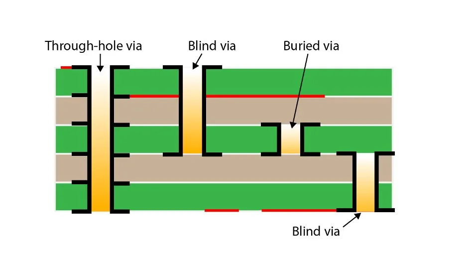
Understanding Blind Vias and Via Stitching in Grounding
Blind vias differ from traditional through vias by terminating at an inner layer rather than penetrating the entire board thickness, allowing for higher routing density and optimized layer usage in multilayer PCBs. In grounding techniques, they connect surface components or traces directly to adjacent ground planes, preserving space and reducing parasitic effects. Via stitching involves placing multiple blind vias in a pattern to interconnect split or segmented ground planes, ensuring a distributed low-inductance path for return currents. This method addresses common issues like ground bounces and voltage drops that arise in high-frequency operations. By strategically positioning these vias, engineers can form a robust ground network that supports EMI control without unnecessary board real estate consumption. IPC-2221 provides foundational guidelines for designing such vias, emphasizing aspect ratios and plating requirements to ensure reliability.
The Mechanisms Behind Noise in PCBs and the Role of Grounding
Noise in PCB design originates from sources such as switching transients, crosstalk between traces, and impedance discontinuities at layer transitions, all of which degrade signal quality and amplify EMI. Poor grounding creates high-impedance return paths, leading to larger current loops that radiate electromagnetic fields and couple noise into sensitive circuits. Solid ground planes offer the lowest inductance, but splits or gaps in these planes introduce slots that act as antennas, exacerbating radiated emissions. Blind vias mitigate this by stitching across these splits, providing multiple parallel paths that lower overall impedance and confine fields. The return current follows the path of least impedance, so densely placed blind vias near high-speed signals ensure tight coupling and minimal loop areas. Effective implementation of these grounding techniques directly correlates with improved noise reduction across the frequency spectrum.
Technical Principles of EMI Control Using Blind Vias
Electromagnetic interference in PCBs arises from both conducted and radiated coupling, where fast edges on signals generate broadband noise that propagates through power and ground structures. Grounding techniques with blind vias excel by creating short, direct return paths adjacent to signal vias, reducing the enclosed area that determines radiated field strength. In multilayer boards, blind vias target specific layer pairs, avoiding unnecessary stubs that could resonate and amplify EMI at quarter-wave frequencies. Via stitching patterns, often arranged in fences or grids, form a Faraday cage-like barrier around sensitive areas, attenuating external noise ingress. The inductance of a via stitch array decreases inversely with the number and proximity of vias, enabling better high-frequency performance. Adhering to IPC-6012 performance specifications ensures these structures withstand thermal and mechanical stresses without degrading over time.
Engineers must consider the skin effect at gigahertz frequencies, where currents concentrate on plane surfaces, making surface-to-inner-layer blind vias particularly effective for stitching. This configuration minimizes via stub lengths, which otherwise act as resonators contributing to EMI peaks. Simulations reveal that stitching with blind vias spaced appropriately around IC perimeters can reduce peak emissions by maintaining plane integrity. The choice of blind over buried vias allows access from both sides if needed, enhancing flexibility in grounding schemes. Overall, these principles form the backbone of robust EMI control strategies in PCB design.
Best Practices for Implementing Blind Vias in Grounding Techniques
Start with a dedicated ground plane strategy, assigning inner layers to continuous ground pours while using blind vias to bridge any necessary splits for power isolation. Place stitching vias adjacent to every signal via that transitions layers, ensuring the return path remains within millimeters to minimize loop inductance. For EMI control, align blind via patterns along board edges and around high-speed sections, creating a perimeter fence that blocks slot radiation. Consult manufacturer capabilities for blind via aspect ratios, typically limited to 1:1 or better for laser-drilled types, to avoid plating voids. Integrate these vias early in the layout process, using grid-based placement tools for uniform density without overlapping other features.
In dense designs, combine blind vias with microvias for finer stitching where space constrains standard drills. Verify ground net continuity through design rule checks, focusing on net impedance and plane coupling. IPC-4761 outlines via protection methods, recommending filled or capped blind vias in environments prone to reliability issues like thermal cycling. Test prototypes with near-field probes to validate noise reduction, adjusting stitch density based on observed emissions. Document via schedules specifying drill depths and lands to streamline fabrication. These practices ensure scalable grounding techniques that enhance overall PCB performance.
Troubleshooting Grounding Issues with Blind Vias
Common pitfalls include insufficient stitch density leading to persistent ground bounces, observable as ringing on oscilloscope traces during load switching. If EMI scans show peaks at board edges, add blind via fences with spacing scaled to the highest operating frequency. Fabrication misalignment can cause open stitches; mitigate by specifying sequential lamination processes for precise blind via registration. In stacked designs, verify no unintended shorts between non-adjacent grounds via cross-section analysis. Power integrity simulations help predict voltage droops, guiding additional stitching near power pins. Addressing these systematically restores effective noise reduction and EMI control.
Conclusion
Blind vias revolutionize grounding techniques in PCB design by enabling targeted via stitching that delivers low-impedance paths and superior EMI control. These structures address the core mechanisms of noise generation, from return path discontinuities to radiated loops, fostering reliable high-speed operation. By following structured best practices and leveraging standards like IPC guidelines, engineers achieve measurable noise reduction without compromising density. Integrating blind vias thoughtfully into multilayer stacks optimizes both signal integrity and thermal management. As PCB complexities grow, mastering these methods remains essential for robust, compliant designs. Prioritize continuous ground planes augmented by strategic stitching for optimal performance.
FAQs
Q1: What are the primary benefits of using blind vias for via stitching in grounding techniques?
A1: Blind vias provide layer-specific connections that reduce stub lengths and loop inductances, crucial for noise reduction in multilayer PCBs. They enable dense stitching patterns without penetrating the full stack, minimizing EMI radiation from ground splits. This approach maintains signal integrity at high frequencies while preserving routing space. Proper implementation aligns with PCB design standards for reliable performance.
Q2: How does via stitching with blind vias contribute to EMI control?
A2: Via stitching creates multiple parallel return paths, lowering impedance and confining electromagnetic fields to reduce radiated emissions. Placed near signal transitions, blind vias ensure current follows tight loops, preventing slot antennas in ground planes. This technique effectively suppresses crosstalk and external noise coupling in high-speed PCB design. Engineers observe improved compliance in EMI testing after optimization.
Q3: What spacing guidelines apply to blind via stitching for noise reduction?
A3: Spacing depends on frequency, with denser patterns near high-speed areas to achieve lambda/20 intervals for optimal EMI control. General rules suggest vias every few millimeters along splits, balanced against fabrication limits. This ensures uniform ground potential and minimizes inductance variations. Adjust based on simulation and prototype validation for specific PCB designs.
Q4: When should electric engineers choose blind vias over through vias for grounding?
A4: Opt for blind vias in dense multilayer boards where through vias waste inner layer space and introduce stubs that resonate. They excel in targeted stitching for EMI control and noise reduction without full-board penetration. Use through vias for simpler, cost-effective stitching in fewer layers. Selection hinges on stackup requirements and performance needs.


