 ALLPCB


Introduction
High-speed clock oscillators form the backbone of modern digital systems, driving everything from data converters to high-speed serial links. Jitter in these oscillators introduces timing uncertainties that propagate through the circuit, compromising overall performance. High speed clock oscillator jitter becomes particularly problematic at frequencies above 100 MHz, where even picosecond deviations can lead to signal degradation. Engineers must address this through targeted oscillator jitter reduction techniques centered on PCB design choices. This article delves into practical strategies for minimizing jitter via power supply optimization, layout refinements, and thermal management. By implementing these methods, designers can achieve reliable operation in demanding applications like telecommunications and computing.
Understanding Jitter in Clock Oscillators
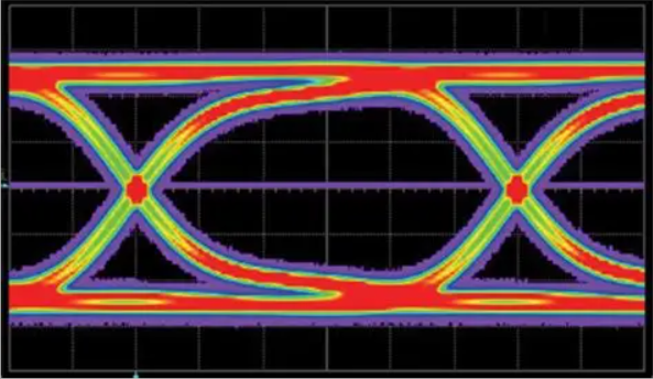
Jitter refers to the deviation of a clock edge from its ideal position in time, manifesting as short-term variations in period or phase. Common types include period jitter, which measures cycle-to-cycle deviations over thousands of cycles, cycle-to-cycle jitter as the maximum difference between adjacent periods, and timing interval error tracking edge positions against an ideal reference. Phase jitter, often specified in the frequency domain, accumulates over multiple cycles and directly impacts signal-to-noise ratio in receivers. JEDEC JESD65B provides standardized definitions for these metrics, ensuring consistent evaluation across devices. In high-speed systems, excessive jitter closes the eye diagram, reducing eye height and width, which signals poor signal integrity. Understanding these mechanisms is essential before applying oscillator jitter reduction techniques.
Why does jitter matter? It directly erodes timing margins in synchronous systems, increasing bit error rates in SerDes interfaces and degrading effective number of bits in ADCs. For instance, random jitter sources like thermal and flicker noise add uncorrelated variations, while deterministic components from reflections exacerbate the issue. In PCB environments, these effects compound with layout parasitics. Minimizing high speed clock oscillator jitter ensures compliance with stringent timing budgets. Ultimately, low-jitter clocks enable higher data rates and system reliability.
Primary Causes of Jitter in High-Speed Oscillators
Power supply noise stands as a leading contributor to oscillator jitter, where voltage ripple couples into the oscillator core, modulating its frequency. Switching transients from digital loads create ground bounce, further destabilizing the supply rails. PDN impedance discontinuities amplify high-frequency noise, converting it into phase perturbations. Crosstalk from adjacent traces induces deterministic jitter via capacitive and inductive coupling. Signal reflections arise from impedance mismatches, causing ringing that smears clock edges.
Environmental factors like temperature fluctuations alter crystal resonance and varactor tuning, introducing long-term drift. Dielectric losses in PCB materials attenuate high-frequency content, acting as a low-pass filter and worsening jitter with trace length. EMI from external sources penetrates shields, adding periodic components. Random jitter stems from intrinsic noise mechanisms such as shot noise in semiconductors. Identifying these causes guides effective mitigation strategies.
Oscillator Power Supply Filtering Techniques
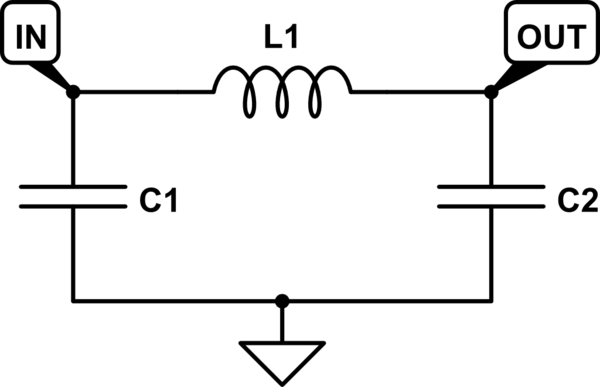
Effective oscillator power supply filtering isolates the clock from PDN noise, a cornerstone of jitter reduction. Place multiple decoupling capacitors directly at the oscillator power pins, combining low-ESR ceramic types like 0.1 μF for high frequencies with larger electrolytic or tantalum for bulk storage. This combination shunts noise across a broad spectrum, stabilizing the voltage. Implement LC pi-filters between the main supply and oscillator, using inductors or ferrite beads to block high-frequency components while passing DC. Dedicated low-noise linear regulators provide cleaner rails than switching types, minimizing ripple injection.
Separate analog and digital power planes prevent cross-domain noise coupling, with stitching vias tying grounds. Ferrite beads in series with the supply offer high impedance at oscillator harmonics, attenuating conducted noise. Verify filter effectiveness through PDN impedance profiling to ensure low impedance up to the clock frequency. These oscillator power supply filtering practices can reduce phase noise by orders of magnitude. Consistent application yields measurable jitter improvements in prototypes.
Optimizing PCB Layout to Minimize Oscillator PCB Layout Jitter
PCB layout profoundly influences high speed clock oscillator jitter through parasitics and coupling paths. Employ full solid ground planes beneath the oscillator to provide low-inductance return paths and shield against EMI. Route clock traces as short as possible with controlled 50-ohm impedance, using width and spacing per IPC-2221B guidelines to match characteristic impedance. Minimize vias on clock nets, opting for blind or buried types if multilayer routing demands them. Symmetric routing for differential clocks preserves balance and rejects common-mode noise.
Terminate clock traces appropriately: series resistors at the driver for source matching or parallel at receivers to absorb reflections. Guard traces or grounded coplanar waveguides isolate clocks from parallel high-speed signals, curbing crosstalk. Avoid routing over plane splits, which create inductive loops amplifying ground bounce. IPC-2221B emphasizes conductor spacing to prevent unintended coupling in dense layouts. Post-layout simulations confirm impedance continuity and jitter budgets.
Enhancing Oscillator Temperature Stability
Temperature variations induce frequency drift in quartz oscillators, manifesting as low-frequency jitter components. Select temperature-compensated crystals (TCXOs) for inherent stability, or oven-controlled types for ultra-precision needs. On the PCB, surround the oscillator with thermal vias and copper pours to equalize heat flow, preventing localized hotspots. Low-temperature-coefficient dielectrics and laminates maintain consistent dielectric constant across operating ranges.
Position the oscillator away from power-dissipating components like voltage regulators or processors. Incorporate thermal relief pads under the package to balance solder joint stress without impeding heat sinking. Monitor stability via aging tests, accounting for initial drift. Oscillator temperature stability directly correlates with long-term jitter performance in varying environments. These measures ensure compliance with system timing over -40°C to 85°C ranges.
Advanced Oscillator Jitter Reduction Techniques
Beyond basics, integrate jitter-cleaning PLLs downstream of the oscillator to filter input noise while multiplying frequency. Pre-emphasis at the driver boosts high-frequency content, countering trace losses. Clock buffers with low additive jitter distribute signals without degradation. Frequency planning avoids harmonics overlapping sensitive bands. Comprehensive SI simulations predict total jitter, including contributions from all sources.
Hybrid approaches combine filtering with layout symmetry for synergistic gains. Field testing with spectrum analyzers quantifies phase noise conversion to time domain. Iterative prototyping refines these techniques.
Conclusion
Reducing high speed clock oscillator jitter demands a holistic approach encompassing power supply filtering, meticulous PCB layout, and thermal management. Key takeaways include strategic decoupling, solid ground planes, impedance control, and temperature-aware placement. Adhering to standards like IPC-2221B and JEDEC JESD65B ensures robust designs. Implementing these oscillator jitter reduction techniques empowers engineers to meet aggressive timing specs. Future systems will rely on even tighter jitter budgets, underscoring the value of these practices.
FAQs
Q1: What are the most effective oscillator power supply filtering techniques for high speed clock oscillator jitter reduction?
A1: Oscillator power supply filtering starts with multi-value decoupling capacitors at the pins, such as 0.1 μF ceramics paired with 10 μF for broadband noise suppression. LC pi-filters with ferrite beads block high-frequency ripple from reaching the core. Dedicated low-noise regulators and separate planes prevent digital noise coupling. These methods stabilize voltage, converting less noise to phase jitter per JEDEC JESD65B metrics.
Q2: How does PCB layout impact oscillator PCB layout jitter in high-speed designs?
A2: Solid ground planes under the oscillator provide return paths and shielding, minimizing inductive noise. Controlled-impedance traces with proper termination eliminate reflections, a major deterministic jitter source. Short routing, via minimization, and isolation from noisy nets reduce crosstalk. IPC-2221B spacing rules prevent coupling, ensuring low oscillator PCB layout jitter across frequencies.
Q3: Why is oscillator temperature stability critical for jitter performance?
A3: Temperature shifts alter crystal frequency via thermal expansion and doping changes, introducing drift jitter. Thermal vias and copper balancing prevent gradients around the oscillator. Low-CTE materials maintain dielectric consistency. Oscillator temperature stability preserves phase noise specs over wide ranges, vital for reliable high-speed operation.
Q4: What role do industry standards play in oscillator jitter reduction techniques?
A4: Standards like JEDEC JESD65B define jitter types and measurement, guiding verification. IPC-2221B provides layout rules for impedance and spacing, curbing layout-induced jitter. They ensure designs meet performance without over-specification. Consistent adherence streamlines qualification and interoperability.
References
IPC-2221B — Generic Standard on Printed Board Design. IPC, 2003
JEDEC JESD65B — Definition of Skew Specifications for Standard Logic Devices. JEDEC, 2009
IPC-6012E — Qualification and Performance Specification for Rigid Printed Boards. IPC, 2017


