ALLPCB


Introduction
Signal integrity remains a critical concern in high-speed digital designs where data rates continue to increase. Even small timing differences between signals can lead to errors, reduced margins, or complete system failures. PCB stackup plays a central role in controlling propagation characteristics across layers and within differential pairs. Engineers must balance electrical performance, manufacturability, and cost when planning layer arrangements and material selections. Effective stackup strategies address both global length matching and localized variations caused by substrate properties. These approaches help maintain consistent signal timing from transmitter to receiver.
Understanding Signal Skew and Its Impact
Signal skew refers to the difference in arrival times between related signals, particularly within differential pairs or between clock and data lines. In high-speed digital PCB design, even picosecond-level mismatches can degrade eye diagrams and increase bit error rates. Skew arises from variations in propagation velocity, which depends on trace geometry, dielectric properties, and copper roughness. PCB stackup for minimizing signal skew focuses on creating uniform electrical environments across critical nets. Without proper attention during layout, these timing differences accumulate and limit achievable data rates. Industry standards such as IPC-2221 guide general design practices that support controlled impedance and timing requirements.
Primary Causes of Signal Skew
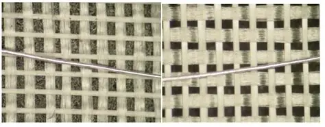
The glass weave effect represents one of the most significant contributors to intra-pair skew in fiberglass-reinforced laminates. Woven glass fibers create periodic regions of higher and lower dielectric constant depending on whether traces run parallel or perpendicular to the weave. This anisotropy causes one leg of a differential pair to experience a slightly different effective permittivity than the other, resulting in velocity mismatch. Additional factors include asymmetric layer stackups that place traces at different distances from reference planes, variations in resin content, and copper foil profiles that affect insertion loss differently across pairs. Temperature and humidity can further modulate these effects during operation. Understanding these mechanisms allows designers to target root causes rather than applying only corrective routing techniques.
Advanced Stackup Design Principles
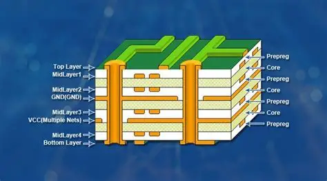
Symmetric stackups form the foundation for minimizing skew by ensuring balanced copper distribution and dielectric thicknesses above and below signal layers. Placing high-speed differential pairs on layers with identical constructions relative to their reference planes helps equalize propagation delays. Engineers often incorporate multiple ground planes to provide consistent return paths and reduce crosstalk that could indirectly affect timing. Careful selection of core and prepreg thicknesses allows fine-tuning of impedance while maintaining overall board flatness. Rotating adjacent signal layers by 90 degrees or using spread-glass fabrics reduces the alignment of traces with weave patterns. These structured decisions during stackup planning limit the need for extensive post-layout compensation.
Laminate Selection for Skew Control
Laminate choice directly influences dielectric uniformity and therefore skew performance. Materials with lower and more stable dielectric constants across frequency and temperature ranges support tighter timing control. Spread-glass or mechanically spread reinforcements minimize the periodic variations associated with conventional weaves. Lower resin-content systems or those using alternative reinforcements can further reduce anisotropy. When selecting materials, designers evaluate not only nominal Dk values but also consistency lot-to-lot and within a panel. IPC-6012 specifications provide qualification criteria that help ensure laminates meet the electrical and physical requirements for high-speed applications. Combining appropriate laminates with optimized stackup symmetry yields better results than either approach alone.
Signal Skew Correction Techniques
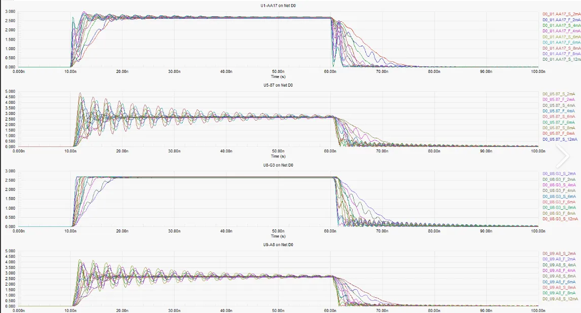
Even with optimized stackups, minor residual skew may remain and require correction. Length matching within pairs through meandering or trombone routing compensates for velocity differences, though this must be done without introducing excessive impedance discontinuities. Some designs employ active deskew circuits or programmable delay elements on the silicon side. At the board level, careful via placement and back-drilling reduce stubs that can cause reflections and apparent timing shifts. Pre-layout simulation using accurate material models helps predict skew before fabrication. Post-layout extraction and adjustment further refine performance. These methods work best when the initial stackup already minimizes the magnitude of correction needed.
Practical Implementation Guidelines
Begin stackup development by defining target impedances and allowable skew budgets based on system timing analysis. Collaborate early with fabricators to confirm achievable tolerances for dielectric thickness and copper weights. Document material assignments and layer orientations clearly in fabrication drawings. Perform signal integrity simulations that incorporate realistic glass-weave models rather than assuming isotropic dielectrics. Review stackup symmetry for both electrical and mechanical balance to avoid warpage that could indirectly affect high-speed performance. Validate prototypes through TDR and eye diagram measurements to confirm skew remains within specifications. Iterative refinement between design and manufacturing feedback improves outcomes on subsequent builds.
Conclusion
Advanced stackup techniques provide a proactive means to control signal skew in high-speed digital PCB design. By addressing glass weave effects through material and orientation choices, maintaining symmetry, and applying targeted corrections, engineers achieve reliable timing performance. These methods integrate with established industry practices to deliver both electrical and manufacturing robustness. Consistent application of these principles supports higher data rates while reducing the risk of costly respins. Ultimately, thoughtful stackup planning remains essential for meeting the demands of modern electronic systems.
FAQs
Q1: What is the glass weave effect in PCB stackup for minimizing signal skew?
A1: The glass weave effect occurs when differential pair traces interact differently with the periodic structure of woven glass reinforcement in the laminate. One trace may overlie more glass while the other overlies more resin, creating a localized dielectric constant difference that produces velocity mismatch and intra-pair skew. Careful laminate selection and layer rotation help mitigate this phenomenon in high-speed digital PCB design.
Q2: How does laminate selection influence signal skew correction?
A2: Laminate selection affects the baseline uniformity of dielectric properties across a panel. Materials with spread glass or more homogeneous constructions reduce inherent anisotropy that contributes to skew. When combined with symmetric stackups, these choices lower the amount of corrective routing or compensation required later in the design process.
Q3: Why is stackup symmetry important for high-speed digital PCB design?
A3: Symmetric stackups place critical signal layers in equivalent positions relative to reference planes and maintain balanced copper distribution. This approach equalizes propagation characteristics and minimizes differences in delay between pairs or between layers. It also supports better mechanical stability during manufacturing and operation.
Q4: What role do industry standards play in PCB stackup planning?
A4: Standards such as IPC-6012 establish qualification and performance requirements for rigid printed boards, including criteria relevant to dielectric materials and construction. Following these guidelines helps ensure that stackup designs meet electrical and reliability expectations for high-speed applications while remaining manufacturable.
References
IPC-2221B — Generic Standard on Printed Board Design. IPC, 2012
IPC-6012E — Qualification and Performance Specification for Rigid Printed Boards. IPC, 2017
IPC-A-600K — Acceptability of Printed Boards. IPC, 2020