 ALLPCB


Introduction
Six-layer printed circuit boards represent a significant advancement in multilayer PCB technology, enabling complex routing for high-performance electronics. These boards feature six copper layers separated by dielectric materials, providing dedicated planes for signals, power, and ground to enhance signal integrity and reduce electromagnetic interference. The fabrication process for 6-layer PCBs demands precision at every stage due to the increased layer count and tighter tolerances compared to simpler two- or four-layer designs. Engineers rely on this process to achieve reliable performance in applications like telecommunications, automotive systems, and computing hardware. Understanding the 6-layer PCB fabrication process ensures designs translate effectively from simulation to production. This guide details the key manufacturing steps, focusing on critical operations such as drilling, etching, plating, and solder mask application.
What Is a 6-Layer PCB and Why Fabrication Matters
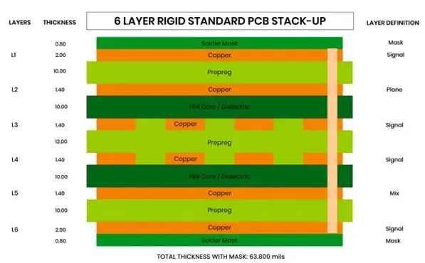
A 6-layer PCB consists of six conductive copper layers embedded within a rigid substrate, typically FR-4 material, with prepregs bonding the layers during lamination. Common stackups include signal-ground-power-signal-power-ground configurations to optimize impedance control and thermal management. Fabrication matters because multilayer boards like these support higher component densities and faster signal speeds, critical for modern electric engineering projects. Poor execution in manufacturing can lead to issues such as via failures, layer misalignment, or excessive warpage, compromising board reliability. Adhering to standards like IPC-6012E ensures qualification and performance specifications are met for rigid printed boards. For electric engineers, mastering these processes facilitates better design-for-manufacturability decisions and reduces iteration costs.
The relevance extends to quality control, where factory insights emphasize sequential buildup to maintain interlayer registration. Engineers must consider aspect ratios and material properties early to avoid fabrication pitfalls. This structured approach aligns production with design intent, supporting applications requiring robust power distribution and minimal crosstalk.
Overview of the 6-Layer PCB Fabrication Process
The 6-layer PCB fabrication process begins with panel preparation and inner layer patterning, progressing through lamination, via formation, and final finishing. Inner layers are etched first on double-sided copper-clad laminates, then aligned and pressed with prepregs under heat and pressure to form the multilayer core. Through-holes are drilled post-lamination to interconnect layers, followed by chemical and electrolytic plating to deposit copper barrels. Outer layers undergo imaging and etching similar to inners, with solder mask applied for protection. Each step integrates quality checks to verify thickness uniformity and continuity. This sequential workflow demands cleanroom conditions to prevent contamination that could cause shorts or opens.
Factory-driven practices prioritize automation for consistency, especially in high-volume runs. Engineers benefit from understanding these phases to specify tolerances accurately in Gerber files. The process culminates in electrical testing and visual inspection per acceptability criteria.
Inner Layer Preparation and 6-Layer PCB Etching
Inner layer fabrication starts with cutting copper-clad laminates to panel size, followed by application of dry film photoresist on both sides. The panels are exposed to UV light through phototools, developing away unexposed resist to reveal the circuit pattern. Etching removes unwanted copper using alkaline or cupric chloride solutions, leaving traces and pads intact. Post-etch stripping cleans the panels, and an oxide treatment promotes adhesion during lamination. For 6-layer boards, this occurs on multiple core panels, typically three, corresponding to layers 1-2, 3-4, and 5-6. Precise control of etch factors prevents undercutting, ensuring line width fidelity.
The 6-layer PCB etching process requires vigilant chemistry management to maintain etch rates uniform across large panels. Engineers should design with etch compensation in mind, accounting for lateral dissolution during production. This step sets the foundation for reliable interlayer connections.
Lamination and Registration
After inner layer etching, cores receive black oxide or alternative treatments for bond strength. Prepreg sheets, impregnated with resin, are cut and stacked symmetrically with cores in precise alignment using optical pins. The assembly enters a vacuum press at controlled temperature and pressure, curing the resin to fuse layers into a solid panel. X-ray inspection verifies registration accuracy before proceeding. Symmetry in stackup prevents warpage from resin shrinkage differentials. This phase is crucial for 6-layer integrity, as misalignment exceeds tolerances rapidly in multilayers.
Post-lamination, panels undergo routing to final outline if needed. Factory protocols include bake cycles to drive out moisture, aligning with performance specs.
6-Layer PCB Drilling
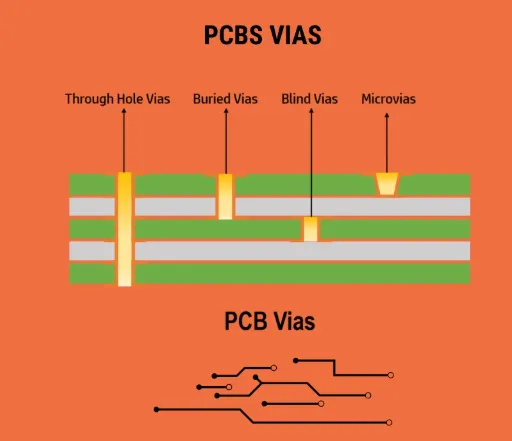
Drilling creates vias and through-holes post-lamination, using CNC machines with carbide or diamond-coated bits for high aspect ratios common in 6-layer boards. Holes range from standard through-vias to blind or buried, with mechanical drilling suiting most production due to speed and cost. Laser drilling supplements for microvias in high-density areas, though hybrid approaches prevail. Entry and exit materials influence breakout quality, demanding optimized feed rates and peck cycles. Aspect ratios up to 10:1 challenge chip removal, necessitating coolant and vacuum extraction. Registration relies on fiducials and X-ray guidance for buried vias.
Quality hinges on hole wall roughness below specified limits to ensure plating adhesion. Engineers optimize drill files with staggered patterns to minimize heat buildup. This 6-layer PCB drilling step directly impacts via reliability in high-speed designs.
Desmear, 6-Layer PCB Plating, and Outer Layer Processing
Desmear follows drilling, using plasma or chemical permanganate to remove epoxy smear from hole walls, exposing fibers for plating grip. Electroless copper seeds the barrels with a thin conductive layer, activated by palladium. Electrolytic plating then builds copper thickness, often via panel or pattern plating methods, followed by tin or nickel for etch resist. Outer layers receive photoresist, imaging, development, and etching akin to inners, stripping resist afterward. The 6-layer PCB plating process ensures barrel integrity per IPC-A-600K acceptability criteria for printed boards. Uniform current distribution prevents dog-boning or voids.
Post-plating, panels undergo profile routing and beveling. Electrical continuity tests confirm plating efficacy before advancing.
6-Layer PCB Solder Mask Application
Solder mask application protects traces from oxidation and solder bridging, applied via screen printing or liquid photoimageable (LPI) methods. LPI offers superior resolution for fine-pitch components, coated uniformly then exposed through artwork, developing away non-image areas. Baking cures the polymer, forming a durable green or alternative color layer. Legend printing follows for component ID using the same process. The 6-layer PCB solder mask application demands precise thickness control, typically 15-25 microns, to avoid via fill issues. Final UV cure enhances hardness and chemical resistance.
Inspection verifies coverage over traces without encroachment on pads. This step integrates with surface finish like HASL or ENIG for assembly readiness.
Best Practices for Successful 6-Layer PCB Fabrication
Select materials with matched CTE to minimize warpage, verifying via stackup simulations. Specify drill margins and plating thicknesses in fab notes to align with capabilities. Implement AOI after etching and plating for defect detection early. Maintain panel size under 18x24 inches for handling stability. Sequential lamination for blind vias enhances density but adds cost, justified by performance gains. Factory insights stress cleanliness protocols, using deionized water rinses throughout.
Engineers should review DFM reports focusing on aspect ratio and annular ring. Pilot runs validate process windows before full production.
Common Challenges in 6-Layer PCB Manufacturing
Warpage arises from asymmetric curing or CTE mismatch, addressed by balanced stackups and constrained pressing. Plating voids stem from poor desmear, mitigated by plasma treatment optimization. Etch undercut in fine lines requires adjusted chemistry and fab feedback loops. Via breakout from drill wander demands entry material backing. Troubleshooting involves cross-section analysis per IPC methods. Proactive design rules prevent most issues.
Conclusion
The 6-layer PCB fabrication process integrates precision etching, drilling, plating, and solder mask application to deliver high-reliability boards for demanding applications. Electric engineers gain from factory-aligned insights, ensuring designs meet performance targets without costly respins. Key to success lies in standards adherence, material selection, and process controls. By understanding these steps, professionals optimize for signal integrity and manufacturability. Future trends point to finer features via advanced plating and laser tech.
FAQs
Q1: What is the 6-layer PCB fabrication process?
A1: The 6-layer PCB fabrication process starts with inner layer etching on cores, followed by lamination with prepregs to form the multilayer stack. Drilling creates interconnecting vias, desmear prepares walls, and plating deposits copper barrels. Outer layers are patterned and etched, concluding with solder mask for protection. This sequence ensures interlayer alignment and electrical continuity, vital for complex circuits. Standards guide each phase for consistency.
Q2: How does 6-layer PCB drilling differ from simpler boards?
A2: In 6-layer PCB drilling, post-lamination holes traverse multiple dielectrics, demanding higher aspect ratios and precise registration via X-ray. Mechanical CNC drills handle through-vias efficiently, while lasers suit microvias. Peck drilling and chip extraction prevent heat damage to inner layers. Quality checks focus on wall roughness for plating adhesion. Engineers specify hit counts per size to optimize tool life.
Q3: What role does plating play in 6-layer PCB fabrication?
A3: Plating in 6-layer PCB fabrication involves electroless copper seeding after desmear, followed by electrolytic buildup for robust via barrels. It interconnects all six layers electrically while maintaining thickness uniformity. Pattern or panel methods suit different densities, with tin resist protecting traces during outer etching. Defects like voids are minimized through current control and chemistry stability. This step is foundational for board functionality.
Q4: Why is 6-layer PCB solder mask application critical?
A4: The 6-layer PCB solder mask application insulates traces, prevents bridging, and protects against environmental factors post-fabrication. LPI processes enable fine resolution matching dense outer layers. Proper thickness avoids impedance shifts or via plugging. Curing ensures mechanical durability for assembly. Inspection confirms pad exposure accuracy, supporting reliable soldering.
References
IPC-6012E — Qualification and Performance Specification for Rigid Printed Boards. IPC, 2017
IPC-A-600K — Acceptability of Printed Boards. IPC, 2020
IPC-2221B — Generic Standard on Printed Board Design. IPC, 2012


