 ALLPCB


Introduction
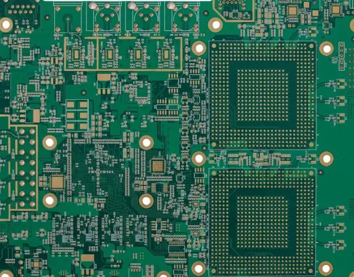
Ball Grid Array (BGA) packages have become essential in modern PCB design with BGAs due to their high pin counts and compact footprints. As electronic devices demand greater performance and smaller sizes, fine-pitch BGA routing presents significant challenges in achieving reliable BGA escape routing. Traditional routing methods often fall short for pitches below 0.8 mm, leading to increased layer counts and routing congestion. Via-in-pad design emerges as a critical technique to address these issues, enabling efficient BGA fanout directly under the package pads. This guide provides electric engineers with a structured approach to implementing BGA via-in-pad design, ensuring optimal signal integrity and manufacturability. By following these steps, designers can enhance PCB design with BGAs while minimizing risks during fabrication and assembly.
What Is Via-in-Pad Design and Why It Matters for BGA Packages
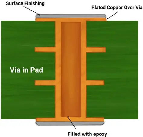
Via-in-pad design places a via directly within the solder land of a surface-mount component, such as a BGA ball pad, rather than offsetting it with a connecting trace. This approach, also known as via-in-pad or VIP, requires the via to be filled, planarized, and overplated to create a flat surface compatible with solder joints. For BGA packages, it eliminates the need for "dogbone" structures, which consume valuable routing space in dense layouts. The technique proves vital for fine-pitch BGAs, where standard through-hole vias would exceed pitch constraints and compromise BGA fanout efficiency.
The relevance stems from the push toward higher integration in applications like processors, FPGAs, and ASICs. Without via-in-pad, designers face routing bottlenecks, higher inductance paths, and thermal management issues during BGA escape routing. It supports denser PCB design with BGAs by allowing signals and power to transition immediately to inner layers, reducing trace lengths and improving electrical performance. Reliability improves as well, since filled vias prevent solder wicking and void formation under the BGA balls. Industry standards like IPC-7095 outline implementation guidelines to ensure these benefits translate to production success.
Technical Principles of Via-in-Pad for BGA Packages
The core principle of via-in-pad revolves around integrating the interconnect seamlessly into the pad geometry while maintaining structural integrity. Vias can be through-hole, blind, or microvias, but for BGAs, laser-drilled microvias or filled through-vias are common to fit within small pad diameters. Aspect ratios must stay below 1:1 for reliable plating, with the via diameter typically 50 to 70 percent of the pad size to provide adequate annular ring. Filling materials include electroplated copper for conductivity or non-conductive epoxy for insulation, followed by planarization to achieve coplanarity within microns.
Plating and capping form the next layer of the mechanism, where copper overplates the filled via to match surrounding pad thickness, typically 0.5 to 1 oz/ft2. This prevents solder flow into the via during reflow, a key concern for BGA assembly. Solder mask application then tents or defines the pad edges precisely. IPC-4761 provides classifications for via protection, such as Type VII for filled and capped vias, which are recommended for via-in-pad under BGAs to enhance reliability against thermal cycling and mechanical stress.
Signal integrity benefits arise from shorter via stubs and lower inductance, crucial for high-speed signals in fine-pitch BGA routing. Thermal dissipation improves as multiple filled vias act as heat conduits to inner planes. However, improper filling can lead to voids or delamination, underscoring the need for controlled fabrication processes.
Step-by-Step Guide to BGA Via-in-Pad Design
Step 1: Assess BGA Package Specifications and Design Requirements
Begin by reviewing the BGA datasheet for pitch, ball diameter, pad size, and pin assignments. Identify critical signals, power/ground nets, and thermal requirements to prioritize fanout strategies. For fine-pitch BGAs under 0.65 mm, confirm via-in-pad necessity, as dogbone routing becomes impractical. Determine layer count and stackup early, allocating inner layers for escape routing. Consult fabrication capabilities for minimum via size and fill options.
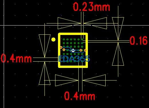
Step 2: Define Pad and Via Geometry
Select pad diameter to accommodate the BGA ball plus annular ring margins per class requirements, ensuring at least 0.1 mm clearance around the via. Position the via centrally in the pad for symmetry. Choose via diameter based on drill feasibility, aiming for an aspect ratio under 0.8:1. Specify fill type: copper for signals/power, epoxy for non-critical vias. Plan for overplating to 15-20 μm thickness.
Step 3: Develop the PCB Stackup for Optimal BGA Fanout
Design a stackup with dedicated signal breakout layers immediately below the BGA. Use 2-4-2 or 3-2-3 configurations for 8-12 layer boards to support dense BGA escape routing. Incorporate plane layers for power integrity and via stitching. Simulate impedance if high-speed, ensuring controlled dielectric thicknesses. Verify HDI compatibility if microvias are used.
Step 4: Implement Via Placement and Initial Fanout
Place vias in pads for perimeter and inner balls, fanning out traces orthogonally to avoid crosstalk. Group power/ground for broadside coupling. Use staggered patterns for ultra-fine pitches to maximize density. Assign nets logically: high-speed to shortest paths, power to multiple vias.
Step 5: Route Escape Traces and Verify Integrity
Route traces on inner layers with minimum widths for current capacity and spacing for isolation. Employ length-matching for differential pairs. Add decoupling caps near power pins. Run DRCs for annular ring, mask clearance, and netlist integrity.
Step 6: Perform DFM and Reliability Checks
Review for solder mask expansion, paste stencil design, and reflow compatibility. Simulate thermal stress per IPC-6012 guidelines. Generate fabrication notes specifying fill, cap, and inspection. Prototype and X-ray inspect for voids.
Best Practices and Common Pitfalls in BGA Via-in-Pad Design
Adhere to consistent via filling across the board to avoid CTE mismatch issues. Prefer copper filling for electrical vias to minimize resistance. Ensure planarization tolerances under 3 μm for reliable BGA joints. During BGA escape routing, prioritize ground vias around signals for shielding.
Common pitfalls include underfilled vias causing head-in-pillow defects or solder voids. Inadequate annular ring leads to pad lift-off. Overlooking stackup symmetry can induce warpage. Always validate with cross-section analysis post-fabrication.
Troubleshooting Via-in-Pad Issues in PCB Design with BGAs
If voids appear in X-rays, check plating chemistry and fill pressure. Delamination signals poor adhesion; verify surface prep. Solder wicking indicates insufficient capping; increase overplate thickness. For routing shorts, inspect mask registration. Thermal failures often trace to aspect ratio violations; redesign with shallower vias.
Iterative testing with thermal cycling per J-STD-001 helps qualify designs. Adjust stencil apertures for better paste volume under filled pads.
Conclusion
Via-in-pad design revolutionizes PCB design with BGAs, particularly for fine-pitch applications demanding efficient BGA fanout and escape routing. By methodically following the outlined steps, engineers achieve higher densities, superior signal integrity, and robust reliability. Key to success lies in precise geometry, proper filling, and stackup planning aligned with standards like IPC-7095 and IPC-4761. Implementing these practices reduces iterations and accelerates time-to-market. Future designs will increasingly rely on this technique as pitches shrink further.
FAQs
Q1: What is BGA via-in-pad design, and when should it be used?
A1: BGA via-in-pad design integrates vias directly into BGA solder pads, filled and capped for flatness. Use it for fine-pitch BGA routing below 0.65 mm pitch where traditional fanout fails due to space limits. It enables direct layer transitions, cutting inductance and boosting density in PCB design with BGAs. Always pair with proper stackup for best results.
Q2: How does via-in-pad improve fine-pitch BGA escape routing?
A2: Via-in-pad eliminates offset traces, freeing space for denser BGA fanout patterns. Filled vias provide low-impedance paths to inner layers, ideal for high-speed signals. It supports routing on fewer layers, simplifying BGA escape routing. Engineers gain better thermal and power distribution without compromising reliability.
Q3: What are key considerations for BGA fanout in via-in-pad layouts?
A3: Prioritize central via placement with adequate annular ring for mechanical strength. Select fill materials matching CTE to prevent cracks. Plan orthogonal trace escapes to minimize crosstalk. Verify DFM for planarization and mask definition to ensure assembly yield.
Q4: Can via-in-pad be used for all BGA pitches in PCB design?
A4: No, it's optimal for fine-pitch BGAs under 0.8 mm; larger pitches may use dogbone instead. Assess based on routing density and layer availability. For ultra-fine pitches, combine with microvias per IPC guidelines. Test for solder joint integrity post-reflow.


