ALLPCB


Overview
Zhongying MCUs integrate a touch module. Touch implementations fall into two categories: those that require an external capacitor C, and those that do not. This article describes usage of the series that requires an external capacitor C.
Typical Application Block Diagram
An external capacitor C1 between 10 nF and 100 nF enables touch detection.
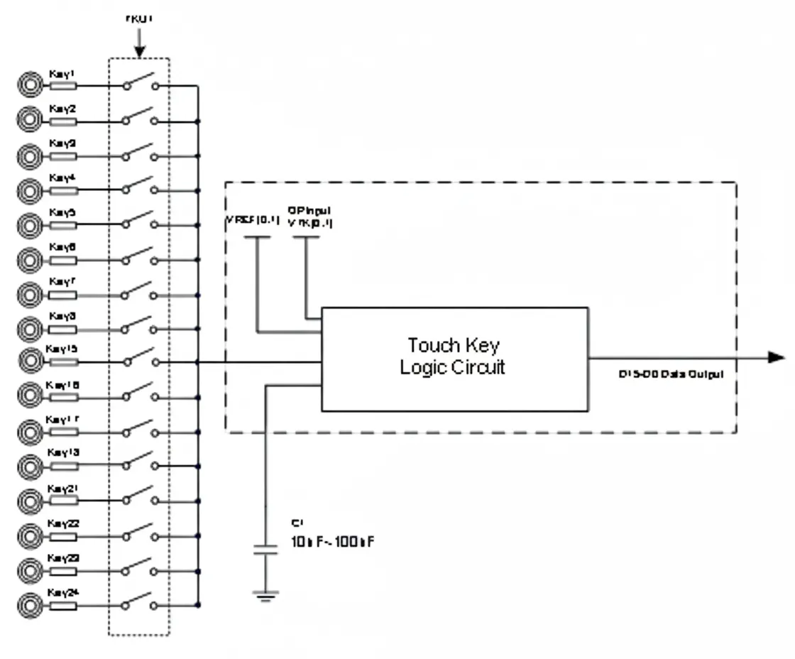
Figure 1-1 Touch application block diagram
Reference Schematic
The reference touch schematic consists of the following parts:
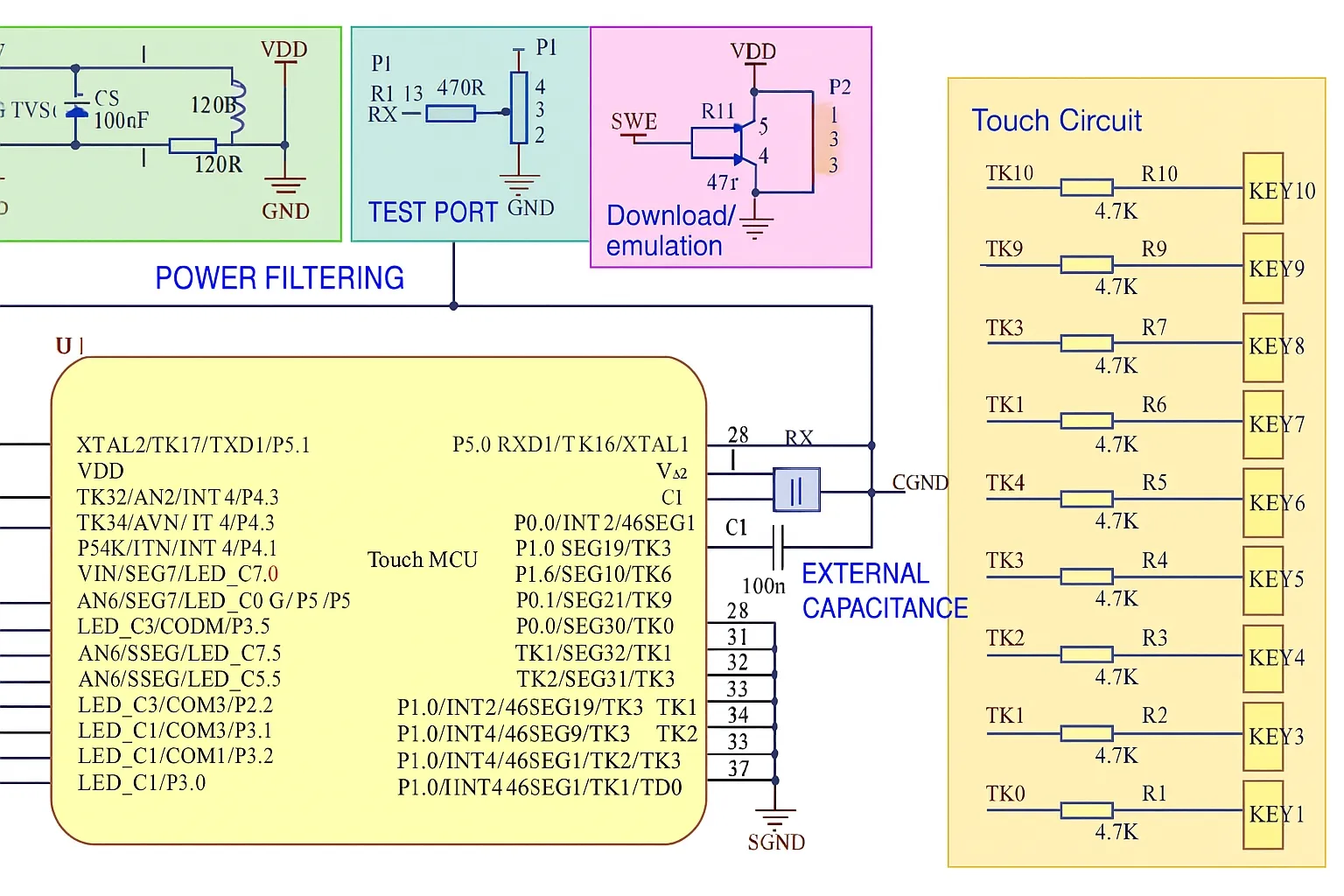
Figure 1-2 Touch reference schematic
Simulation and Debugging
Simulation and debugging notes:
- ISP debug interface pins: VDD, SWE, GND.
- Parameter debug UART interface P1: VDD, RX, TX, GND.
To simplify development, reserve interfaces for debugging and parameter tuning. Zhongying provides the STouch software for observing touch detection data.
Touch Circuit
- External touch capacitor C1: choose a capacitor in the nF range (e.g., 103, 223, 333, 473). Common dielectric types such as X7R are acceptable. For wide temperature ranges (for example down to -30°C), consider NPO capacitors.
- The number of touch pins can be adjusted according to application needs. Where touch pins are configurable, keep them separated from high-frequency IO pins (SPI, I2C, UART, etc.) to simplify PCB routing.
- Place a series anti-interference resistor of 1 kΩ to 4.7 kΩ between the touch pin and the pad; 4.7 kΩ is recommended.
Power Supply
Supply filtering: use bulk and decoupling capacitors, recommended 100 μF + 100 nF + 100 nF. Place the 100 nF close to the power input, and the 100 μF + 100 nF close to the IC. Increasing the number of capacitors on the supply improves noise immunity.
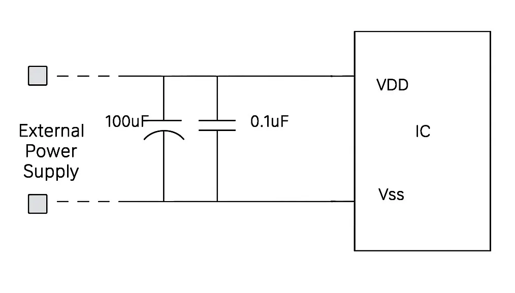
Figure 1-3 Filter capacitor placement
PCB Layout Considerations
To achieve optimal touch performance, follow general PCB routing rules and observe these layout recommendations when drawing the board.
- Place the external touch capacitor C1 and the series resistor close to the MCU pin to improve interference immunity.
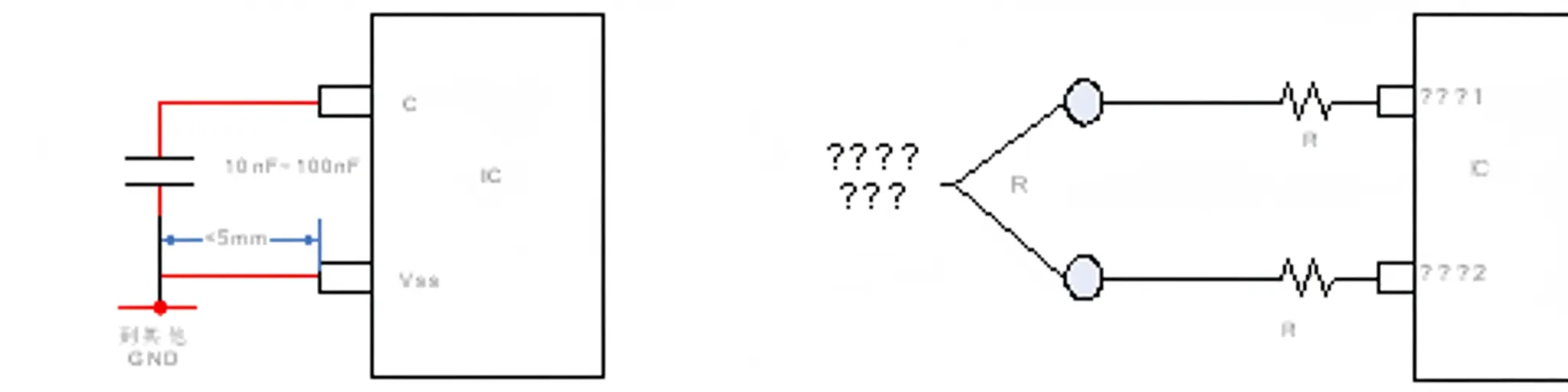
Figure 1-4 Placement of external capacitor C and anti-interference resistor
- Keep spacing between touch traces and between touch traces and other signal traces as large as possible. Parallel distance should be no less than 20 mil; larger spacing is better.
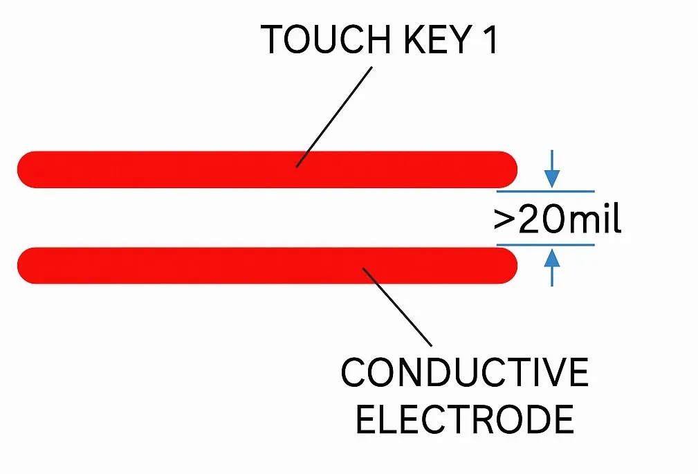
Figure 1-5 Trace spacing
- Capacitive touch keys are high-impedance and are susceptible to interference from high-frequency signal sources (SPI, I2C, UART, PWM, LED, etc.). Avoid routing high-frequency signal traces near touch traces. Do not route the sensing pad-to-chip connection across sources of strong interference or high-frequency traces. If unavoidable, route the traces orthogonally. If parallel routing is necessary due to PCB constraints, include a ground trace between them for isolation.
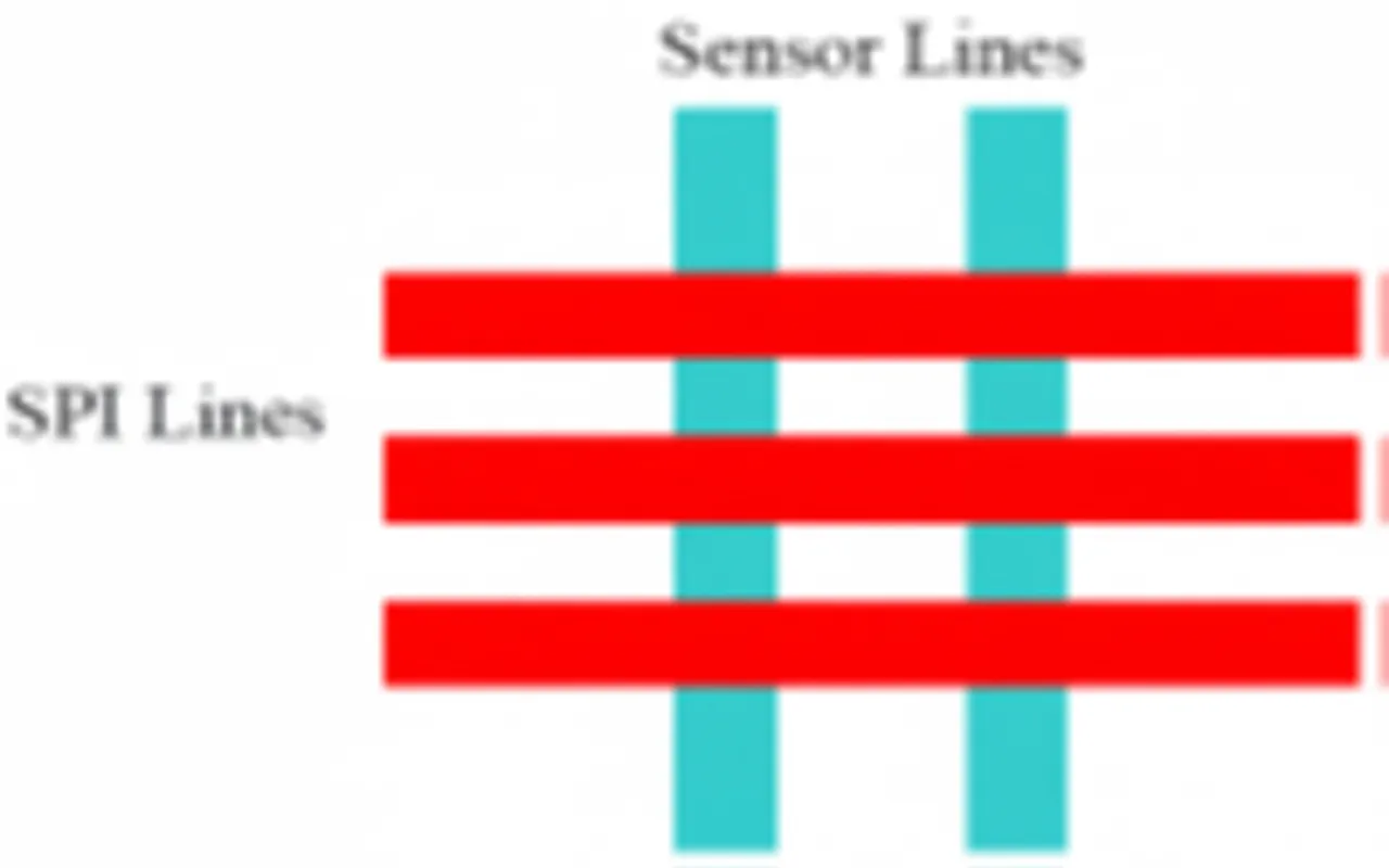
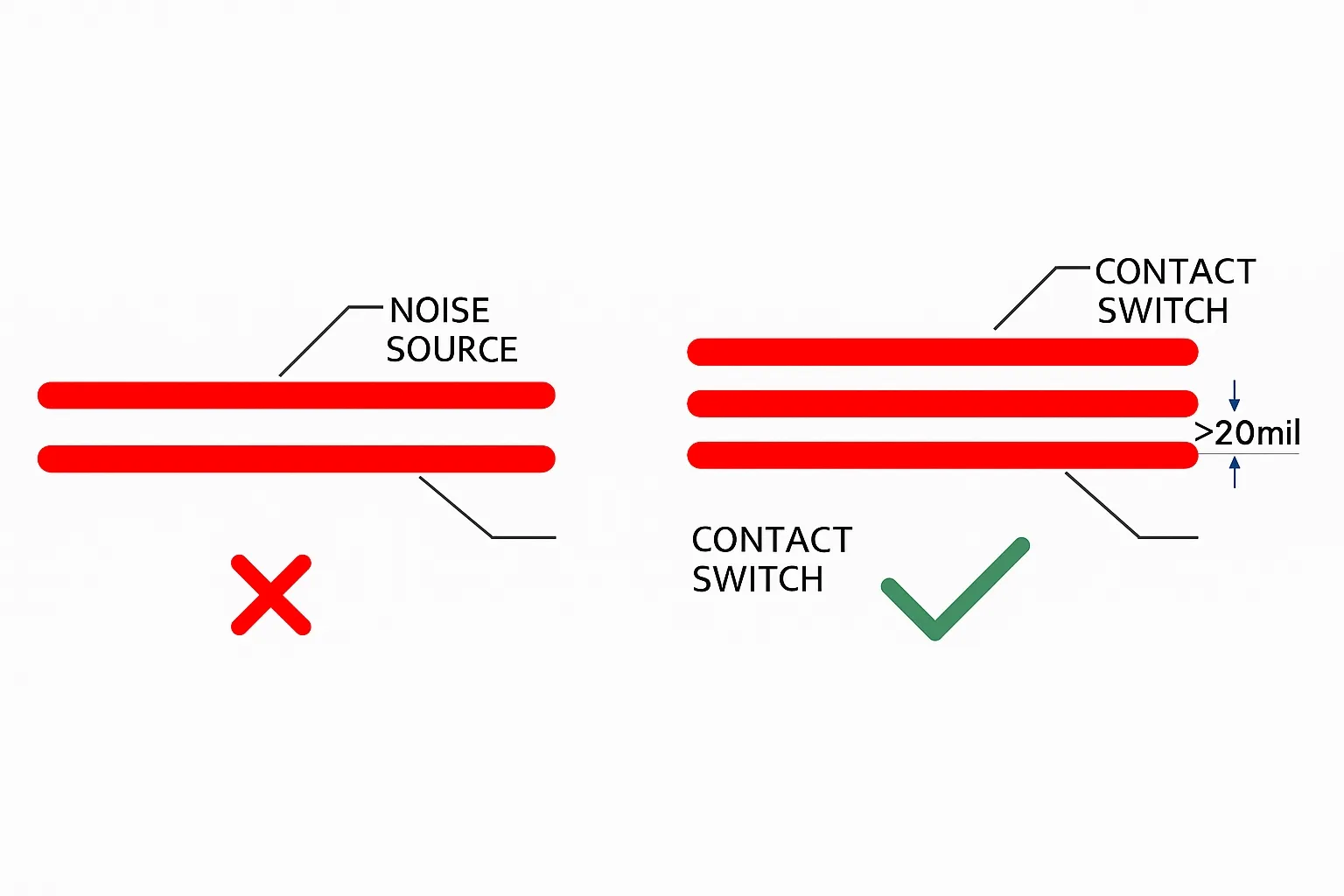
Figure 1-6 Touch key routing and other high-frequency signal routing
- Avoid routing the signal line between the touch pad and the IC close to the PCB edge, as edge interference is higher and the edge is more likely to be touched by a user. For double-sided boards, placing the touch trace on the opposite side from the touch pad can reduce the effect of finger contact on the trace.
- Do not route other touch-key traces beneath a touch key sensor.
Software Configuration
- A touch library with interference mitigation features is available. Users typically only need to set parameters to achieve normal touch operation.
- The STouch software can be used for observing touch data and calibration; it is designed to work with the touch library.
Detailed touch library and STouch software documentation are available.