ALLPCB


Introduction
This article examines recent IEEE Ethernet standards developments and how they address requirements for next-generation hyperscale data centers and AI workloads, with potential gains in performance and scalability.
Key topics
- Brief history of IEEE Ethernet standards
- Updates in IEEE Std 802.3df and IEEE P802.3dj
- Implications for next-generation hyperscale data centers
Context and goals
Building on the original IEEE Std 802.3 first published in 1985, IEEE Std 802.3df and IEEE P802.3dj represent recent progress in Ethernet standards. These new standards pave the way for aggregation link speeds of 200 Gb/s, 400 Gb/s, 800 Gb/s, and 1.6 Tb/s. They target the emerging needs of hyperscale data centers, large language models (LLMs), and machine learning (ML) applications, aiming to improve performance and scalability.
The standards introduce changes across optical and electrical domains, including media access control (MAC), management, and physical layer specifications. In optics, they span single-mode fiber modulation and detection techniques to support physical media attachment (PMA) performance from 500 m with PAM4 signaling to 40 km with DP-16QAM modulation. These specifications extend the supported optical reach and modulation options.
Latest 802.3 standards overview
On the electrical side, the standards establish a new baseline for a single-lane 212 Gb/s interface intended to cover direct-attach copper (CR), chip-to-module (C2M), chip-to-chip (C2C), and backplane (KR) interfaces. The most technically and engineering-challenging electrical interface is the C2M interface, which is the primary physical interface used in QSFP or OSFP module fiber configurations and is central to the development of 104 Tb/s switching technologies. It is a key element for next-generation AI and hyperscale data center interconnects and for upcoming 1.6 Tb/s copper and optical interconnects.
Brief history of recent IEEE standards
Recent and current IEEE standards relevant to this evolution include:
- IEEE Std 802.3ck-2022: Defines per-lane 106 Gb/s physical layers and management parameters for 100, 200, and 400 Gb/s aggregated interfaces.
- IEEE Std 802.3df-2024: Defines MAC and management parameters for 400 and 800 Gb/s aggregated interfaces and reuses the existing per-lane 106 Gb/s physical layer technology.
- IEEE P802.3dj (expected 2025): Defines per-lane 212 Gb/s physical layer and MAC for 1.6 Tb/s aggregated interfaces, and management parameters for 200 Gb/s, 400 Gb/s, 800 Gb/s, and 1.6 Tb/s aggregated interfaces.
Focus on IEEE P802.3dj per-lane 212 Gb/s physical layer
IEEE P802.3dj continues the development cadence of IEEE Std 802.3 to meet demands for higher-speed and more efficient electrical and optical signaling. This article focuses on the developing 212 Gb/s per-lane physical interface. The new interface pushes the limits of electro-optical transmission systems, connector and SerDes design.
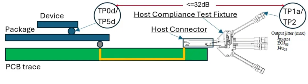
Several channel parameters are built into IEEE P802.3dj. Notably, a channel curve begins at the transmitter chip die-bump test point (TP0d) and ends at the receiver chip die-bump test point (TP5d). The nominal loss between these two test points is 40 dB, with a Nyquist frequency of 53.125 GHz. Figure 1 shows a typical host model that includes TP1a for assessing C2M configurations and TP2 as the passive-cable perspective.
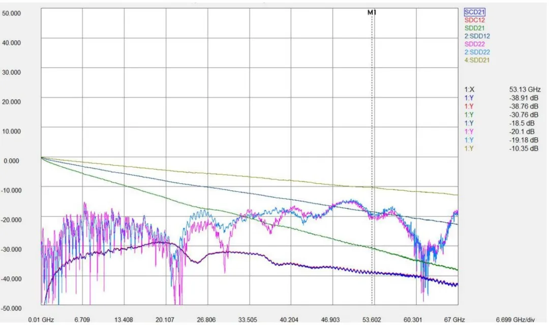
Insertion loss between the die-bump TP0d and TP1a on the silicon may fall within a range of allowed host loss curves that the standard has not fully finalized. A 32 dB net high-loss curve serves as a case study for the electrical validation challenges discussed here. Figure 2 shows these insertion losses and typical return loss parameters for the test structure. The marker at 53.125 GHz indicates the commonly controlled insertion loss limit.
Electrical validation measurements and TP1a
Most electrical validation measurements use TP1a (host output specification). These measurements include common operations such as signal-to-noise-and-distortion ratio (SNDR), steady-state transmitter voltage (Vf), and residual level mismatch (RLM), all of which are included in IEEE P802.3dj (draft) clause 176D for TP1a host output specifications.
IEEE P802.3dj also aligns TP2 cable (CR) test validation with TP1a C2M techniques, recognizing that these are effectively the same test point. For designers familiar with previous generations of C2M technology (53.125 Gb/s PAM4), a notable change in IEEE P802.3dj is the introduction of jitter specifications at the TP1a test point.
Jitter specifications and measurement methodology
Jitter specifications in IEEE P802.3dj derive from earlier techniques that examine a set of 12 strategic edges in the PRBS13Q (PAM4 PRBS13Q) test pattern to extract relevant jitter characteristics. Key jitter metrics include uncorrelated jitter at a 1:104 probability (J4u), uncompensated residual jitter RMS, and even/odd jitter components (EOJ).
Driving fast edge test signals (5 ps transition time) through a combined package, host loss, and test adapter interface with 32 dB attenuation at 53 GHz causes significant lowpass filtering of the signal. The combined filtering and signal memory effects increase inter-symbol interference (ISI) for all single-, double-, and triple-level transitions in PRBS13Q or PRBS9Q streams and reduce edge slew rates. These filtering-induced degradations largely explain measured versus simulated differences.
Specifically, lower slew rates lead to larger jitter values because vertical noise-induced jitter is proportional to noise amplitude divided by edge slew rate. Increased ISI causes greater variation in jitter between different edges. These effects are asymmetric: single-level transitions suffer most (highest jitter and variability), double-level transitions are moderately affected, and triple-level transitions least affected.
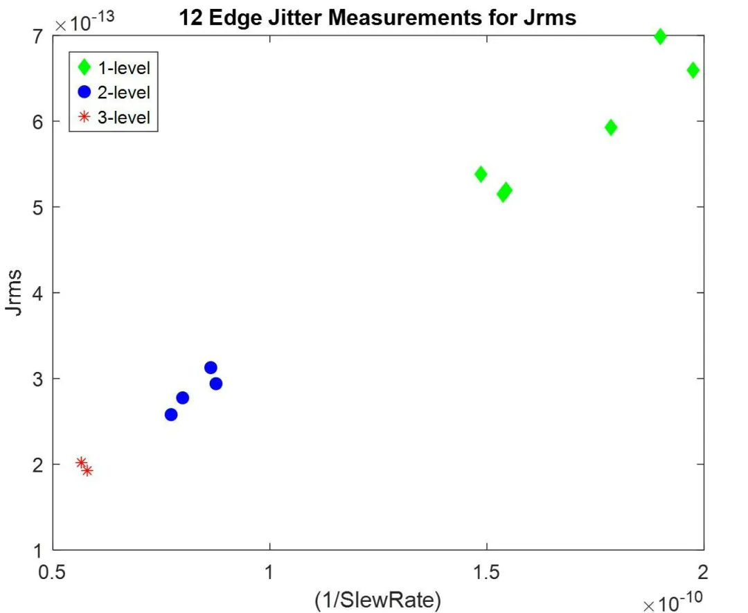
The lower-left triple transition exhibits the lowest JRMS and lowest variability, while the higher (upward and rightward) double and single transitions show higher JRMS and larger variability. This matches observations at the far end of high-loss channels, sometimes called channel-induced jitter amplification. Because of this variability, the current process isolates jitter measurements to triple-level transitions; JRMS03 and EOJ03 symbols originate from this approach.
Latest IEEE 802.3dj proposals
According to the latest proposal D1.3, IEEE 802.3dj offers greater flexibility:
- Jitter can be measured on any triple-level transition. Results are reported separately for rising and falling edges to minimize jitter parameters.
- Tests may use PRBS9Q or PRBS13Q patterns.
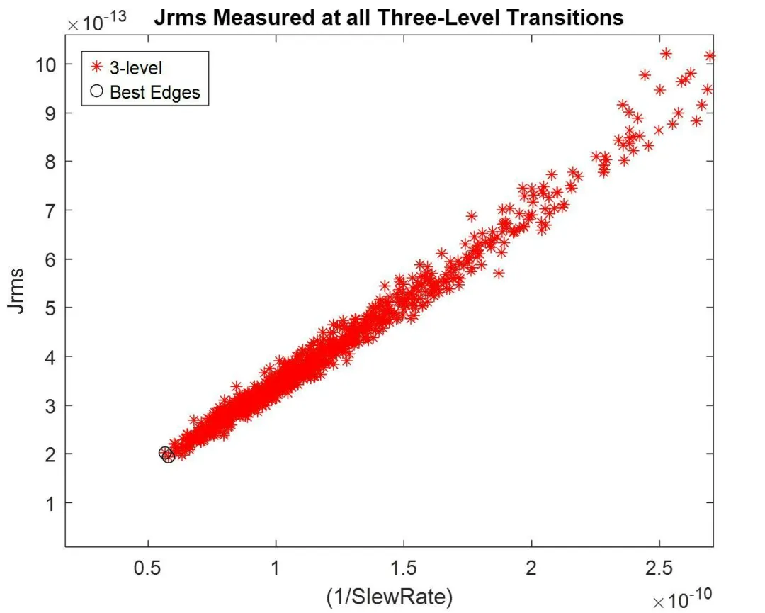
Figure 4 shows JRMS values for all triple-level transitions in a PRBS13Q pattern. The best rising and falling edges are highlighted. Using JRMS03 and the proposed classification focuses attention on transmitter attributes while minimizing the impact of high channel loss.
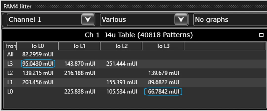
Jitter decomposition and PAM4 transitions
Figure 5 shows a typical physical-layer jitter validation where jitter decomposition traditionally emphasizes all 12 available PAM4 transitions.
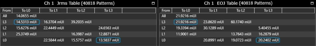
Focusing on triple-level PAM4 transitions, Figure 6 shows JRMS03 and EOJ03. Similar to reporting J4u as the maximum rising or falling triple-level jitter term, this decomposition shows a JRMS03 maximum of 14.5 mUI against a nominal limit of 23 mUI, and an EOJ03 maximum of 21.9 mUI against a nominal limit of 25 mUI.
Implications and conclusion
IEEE Std 802.3df and IEEE P802.3dj jointly mark a significant step in Ethernet evolution, continuing the legacy of the original IEEE Std 802.3. As these standards evolve, they will underpin future high-speed, high-capacity networks and support data-intensive AI workloads, influencing the future direction of Ethernet technologies.