 ALLPCB


Introduction
In PCB design, achieving optimal performance hinges on meticulous planning of the PCB trace routing layout, strategic component placement, and efficient via optimization. These elements directly influence signal integrity, thermal management, electromagnetic compatibility, and overall manufacturability. Electric engineers face constant pressure to balance dense layouts with reliability, especially as board sizes shrink and speeds increase. Poor routing can lead to crosstalk, ground bounce, or impedance mismatches, while suboptimal placement exacerbates these issues by lengthening critical paths. Via overuse compounds problems by introducing inductance and potential failure points under thermal stress. This guide delves into the engineering principles and practical strategies to master these aspects, ensuring designs meet high-reliability demands.
Mastering PCB trace routing layout requires understanding how traces carry signals, power, and ground while minimizing interference. Component placement sets the foundation, dictating trace lengths and congestion. Via optimization then refines connectivity across layers without compromising speed or yield. By following structured approaches aligned with industry standards, engineers can reduce iterations and enhance first-pass success. Whether designing multilayer boards for high-frequency applications or cost-sensitive consumer products, these techniques apply universally.
What Is PCB Trace Routing Layout and Why It Matters
PCB trace routing layout refers to the systematic arrangement of conductive paths on a printed circuit board to interconnect components electrically. Traces vary in width and length based on current carrying capacity, signal speed, and impedance requirements. Routing must account for layer stackup, avoiding sharp bends that cause reflections or manufacturing defects like opens. In high-density designs, autorouters assist but demand manual refinement for critical nets. Component placement profoundly impacts routing feasibility, as misplaced parts create unmanageable fanouts or crossovers.
The relevance of effective PCB trace routing layout cannot be overstated in modern electronics. Suboptimal routing leads to signal degradation, increased power loss, and higher electromagnetic interference, potentially failing compliance tests. For electric engineers, it directly affects product reliability and time-to-market. Dense boards with fine-pitch components amplify challenges, where even minor deviations in trace geometry alter performance. Manufacturability suffers too, with overly complex routes raising costs and defect rates. Prioritizing routing early in the design flow integrates seamlessly with component placement and via strategies, yielding robust boards.
Key Principles of Component Placement in PCB Design
Component placement forms the cornerstone of successful PCB trace routing layout by minimizing trace lengths and reducing layer transitions. Engineers begin by grouping components by function, such as placing decoupling capacitors near power pins to shorten high-frequency loops. Hierarchical placement follows: core analog sections isolated from digital to curb noise coupling, with high-speed signals routed first. Thermal considerations guide placement, separating heat-generating ICs from sensitive analog areas while ensuring airflow paths. Symmetry matters for differential pairs, aligning components to facilitate length-matched routing.
In multilayer boards, vertical alignment across layers optimizes via usage, a critical aspect of via optimization. Place connectors and large components along board edges to ease mechanical assembly and trace escape routing. Density rules dictate spacing: maintain clearances per IPC standards to prevent shorts during fabrication or soldering. Simulate placement early to identify congestion hotspots, adjusting iteratively. This logical sequencing ensures traces flow naturally, preserving signal integrity and easing subsequent routing.
Power and ground planes influence placement profoundly. Position voltage regulators near loads to minimize distribution losses, routing thick power traces alongside. For mixed-signal designs, dedicate zones for RF sections, shielding them with ground pours. Fine-pitch BGA packages demand fanout planning during placement, preallocating escape vias. Overall, thoughtful placement reduces total wire length by up to significant margins, streamlining the entire PCB design process.
Fundamentals of Via Optimization in PCB Trace Routing
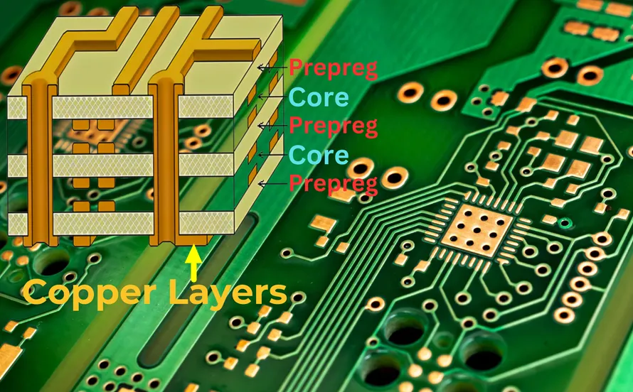
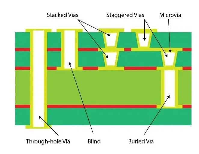
Vias serve as interlayer interconnects but introduce parasitic inductance and capacitance, degrading high-speed signals if overused. Via optimization minimizes their count while ensuring reliable transitions, starting with stackup planning to align signals vertically. Through-hole vias suit power but consume more space; blind and buried types save surface area in high-density boards. Via diameter selection balances drill feasibility with annular ring integrity, adhering to aspect ratio limits for plating uniformity.
Stitching vias enhance return paths for ground planes, placed at regular intervals to lower impedance. In PCB trace routing layout, fanout vias for BGA escape patterns must align with component placement for shortest paths. Microvias enable denser routing in HDI boards, but their higher cost demands judicious use. Optimization techniques include via tentsing to protect against solder wicking and sharing vias for non-critical nets. Per IPC guidelines, via reliability under thermal cycling relies on proper sizing and placement.
Impedance control guides via optimization, with back-drilling removing stubs for high-frequency lines. Simulate via fields to predict crosstalk, adjusting barrel dimensions accordingly. In multilayer stackups, pair signal vias with nearby ground vias to form transmission line equivalents. This reduces reflections and maintains eye diagrams. Effective via strategies integrate with routing rules, preventing bottlenecks.
Best Practices for Integrating Component Placement, Trace Routing, and Via Optimization
Integrate component placement with PCB trace routing layout by locking critical nets early: place high-speed devices first, route their traces, then fill peripherals. Use 45-degree bends over 90-degree for smoother current flow and reduced etch undercuts. Maintain uniform trace widths within nets for consistent impedance, calculating per current and layer thickness. Differential pairs demand length matching within tolerances, often 0.1mm or better, with symmetric routing.
Via optimization pairs with routing by preferring in-pad vias where process allows, minimizing stubs. Employ length-tuning meanders judiciously, avoiding loops that radiate EMI. Ground pours under traces shield against crosstalk, connected via stitching. For power distribution, wide polygons with multiple vias ensure low resistance. Adhere to J-STD standards for solder joint reliability influenced by routing density.
Troubleshoot common pitfalls: excessive vias causing thermal hotspots require redistribution layers. Congested areas from poor placement benefit from jumpers or alternate stackups. Design rule checks enforce min clearances, trace-to-via spacing. Post-layout simulation verifies integrity before fabrication. These practices yield designs compliant with IPC-2221 guidelines for trace geometry and spacing.
Advanced Troubleshooting and Case Insights
In high-speed PCB design, signal integrity issues often trace back to suboptimal component placement forcing long meanders. Engineers troubleshoot by reviewing S-parameters: poor return loss indicates via stub problems. Adjust via optimization with elliptical shapes for better fields in some cases. Crosstalk from parallel traces resolves via guard traces or layer staggering.
A typical multilayer board challenge involves BGA fanout where dense placement congests routing. Solution: microvia transitions with dogbone fanouts aligned to placement grid. Thermal vias under hotspots wick heat, integrated during routing. EMI failures from unshielded edges improve with perimeter stitching. These insights, grounded in engineering logic, prevent redesign loops.
Conclusion
Mastering PCB trace routing layout through strategic component placement and via optimization elevates design reliability and performance. Logical grouping, minimal vias, and impedance-controlled traces form the triad of success. Electric engineers benefit from early simulation and standards adherence, reducing risks. Implement these principles to streamline workflows and achieve superior boards. Future designs will demand even tighter integration as densities rise.
FAQs
Q1: What role does component placement play in PCB trace routing layout?
A1: Component placement dictates trace lengths and congestion in PCB trace routing layout. Group by function to shorten critical paths, isolate noise sources, and align with stackup for via efficiency. This minimizes crosstalk and eases routing, per standard design flows. Early placement simulation identifies issues upfront.
Q2: How can engineers achieve via optimization in dense PCB designs?
A2: Via optimization in PCB design involves minimizing count with blind/buried types and vertical alignment from component placement. Stitch grounds regularly and back-drill for high-speed. Balance size with annular rings for reliability. This preserves surface area and signal quality logically.
Q3: Why is trace width critical in PCB trace routing layout?
A3: Trace width in PCB trace routing layout ensures current capacity and controlled impedance. Narrow traces risk overheating; wide ones cause capacitance. Calculate per layer copper and temp rise, integrating with via transitions. Proper sizing prevents failures under load.
Q4: What are common pitfalls in PCB design via optimization?
A4: Overreliance on through-vias congests boards; poor placement exacerbates this in PCB design. Stub inductance degrades signals. Mitigate with microvias, tentsing, and simulation. Adhere to plating aspect ratios for yield.
References
IPC-2221B — Generic Standard on Printed Board Design. IPC, 2009
IPC-6012E — Qualification and Performance Specification for Rigid Printed Boards. IPC, 2015
J-STD-001H — Requirements for Soldered Electrical and Electronic Assemblies. IPC, 2018


