 ALLPCB


Introduction
Electric engineers designing and assembling printed circuit boards face constant pressure to deliver reliable performance under demanding conditions. Quality control processes directly impact the longevity and functionality of electronic assemblies, particularly in areas like connector testing, soldering integrity, circuit failure prevention, and parts selection for plating. A comprehensive checklist streamlines these efforts, aligning factory operations with proven engineering principles. This guide draws from factory-driven insights to provide actionable steps that minimize defects and enhance reliability. By focusing on standardized methods, engineers can reduce rework costs and accelerate time-to-market. Implementing these tips ensures assemblies meet high-stakes requirements in automotive, aerospace, and consumer electronics applications.

Why Quality Control Matters in PCB Assemblies
Quality control in PCB production serves as the backbone of reliable electronic systems, preventing field failures that could compromise safety and performance. Poorly tested connectors lead to intermittent connections, while subpar soldering causes open circuits or shorts over time. Circuit failures often stem from overlooked contamination or mechanical stress, amplifying risks in high-density boards. Selecting reliable parts for plating ensures optimal solderability and corrosion resistance, extending shelf life. Factory insights reveal that consistent QC adherence boosts yield rates and customer satisfaction. Ultimately, these practices safeguard against costly recalls and uphold engineering reputation in competitive markets.
Adopting a checklist approach standardizes inspections across production lines, fostering repeatability. Engineers benefit from reduced variability, as each step verifies compliance before advancing to assembly. This proactive stance aligns with broader quality management frameworks, emphasizing prevention over correction. In high-volume manufacturing, even minor defects scale exponentially, underscoring the need for meticulous oversight.
Testing Connectors: Essential Methods and Checklist
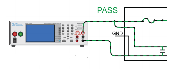
Testing connectors demands thorough electrical and mechanical evaluations to confirm robust interconnections. Begin with visual inspection for alignment, pin damage, and plating integrity, ensuring no bent leads or foreign particles. Electrical continuity tests verify low-resistance paths between mating surfaces, using probes to measure under nominal voltage. Insulation resistance testing, often at 500V DC, detects leakage paths that could cause shorts. Mechanical pull tests assess retention force, simulating vibration stresses common in deployed systems.
Follow a structured checklist: first, confirm connector seating depth per design specs; second, perform hi-pot testing up to 1000V AC for dielectric withstand; third, cycle mate/unmate 50 times to check wear. IPC-A-610 provides criteria for acceptable solder fillet formation around connector pins, guiding visual assessments.Automated optical inspection complements manual checks, flagging misalignments early. Environmental stress screening, like thermal cycling from -40°C to 85°C, reveals latent weaknesses. Document all results for traceability, enabling root cause analysis if issues arise.
In high-reliability applications, flying probe testers offer flexibility for low-volume runs, mapping open circuits precisely. Combine with X-ray for hidden solder voids under shrouded connectors. These methods ensure connectors withstand operational harmonics without signal degradation.
Soldering Best Practices and Materials Selection
Soldering forms the critical junctions in PCB assemblies, where material choices and techniques dictate joint reliability. Select solder alloys compatible with surface finishes, prioritizing lead-free options like SAC305 for modern compliance. Flux selection focuses on no-clean types to minimize residue, ensuring activation without corrosion risks. Preheat boards uniformly to 100-150°C, preventing thermal shock to components. Maintain reflow profiles with peak temperatures around 240-260°C, ramping slowly to avoid defects.
IPC J-STD-001 outlines requirements for materials, process controls, and verification, emphasizing cleanability and joint criteria.Best practices include stencil alignment within 25 microns for paste deposition, followed by immediate reflow. Post-solder cleaning uses isopropyl alcohol ultrasonics to remove activators. Inspect joints for wetting angle under 60 degrees and heel fillet coverage.
Checklist items: verify solder paste viscosity via slump test; monitor voiding below 25% via X-ray; ensure no bridging or icicles. Hand soldering for prototypes demands iron tips at 350°C with ergonomic control. These steps yield void-free, high-strength bonds resistant to fatigue.
Material handling prevents oxidation, storing pastes at 5-10°C with desiccant packs. Nitrogen reflow atmospheres further enhance wetting on fine-pitch parts.
Preventing Circuit Failures: Common Causes and Mitigation Strategies
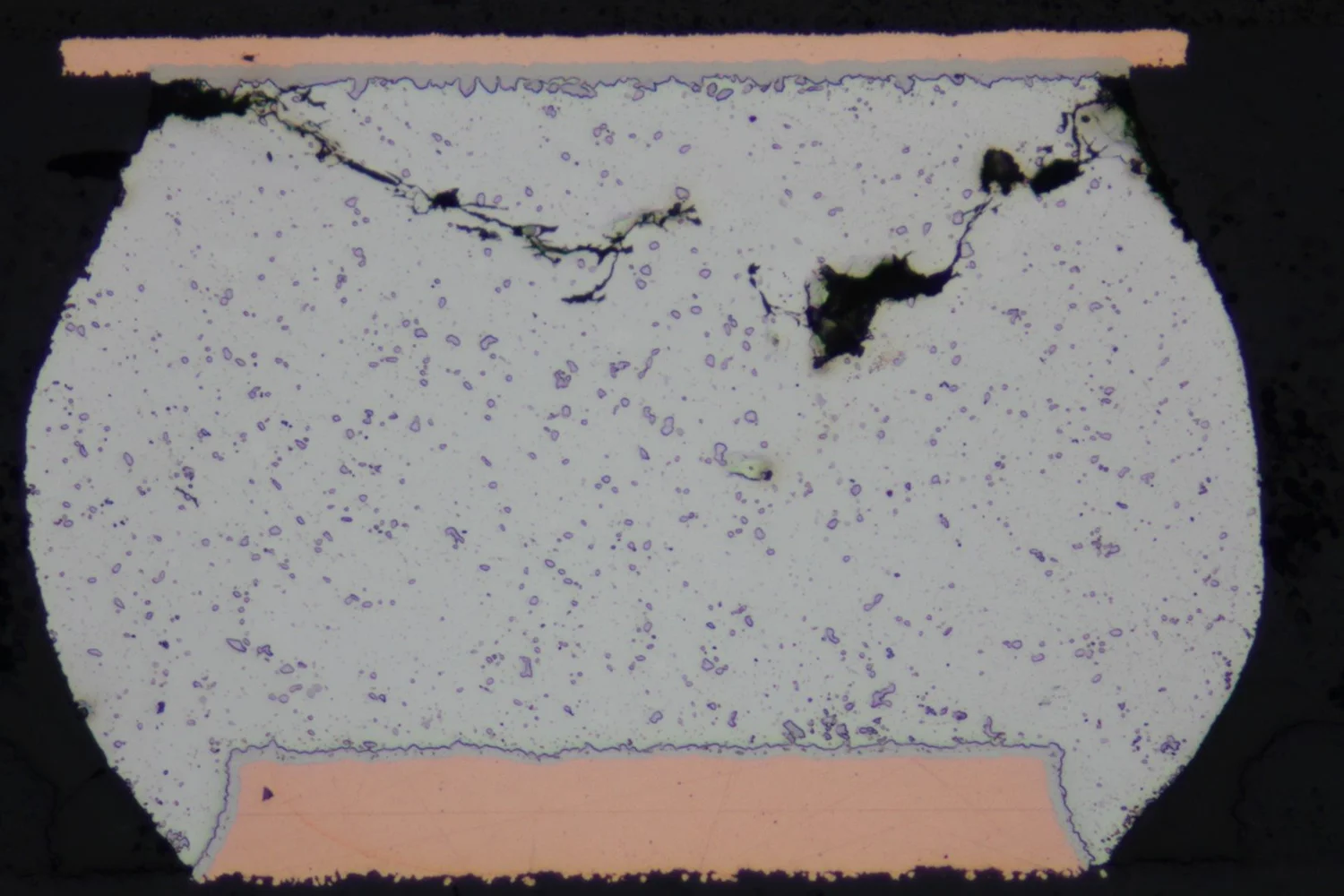
Circuit failures often trace to manufacturing oversights, such as delamination from moisture or cracks from mishandling. Contamination introduces ionic residues, promoting electromigration under bias. Mechanical stress warps boards, fracturing traces during flexure. Thermal mismatches between components and substrate cause fatigue in vias over cycles.
Prevention starts with incoming inspection of laminates per IPC-6012 performance specs, checking for warpage under 0.75%. Bake boards at 125°C for 24 hours pre-assembly to drive out absorbed moisture. Implement automated optical inspection post-etch for trace defects. In-circuit testing verifies nodal voltages and shorts on populated boards.
Key checklist: perform flying probe opens/shorts test; conduct burn-in at 85°C/85% RH for 168 hours; analyze failures via dye penetrant for cracks. Solder mask integrity prevents dendritic growth in humid environments. Vibration testing per IEC standards simulates real-world shocks.
Layered defenses, including functional testing at operating speeds, catch intermittent issues. Traceability logs link defects to processes, enabling continuous improvement.
Reliable Parts Selection for Plating and Surface Finishes
Parts selection for plating prioritizes solderability, corrosion resistance, and compatibility with assembly flows. Evaluate leads and terminations via dip-and-look tests, ensuring 95% wetting coverage. Plating thickness uniformity, typically 2-5 microns for nickel under gold, guards against wear. Immersion finishes like silver demand hermetic sealing post-assembly to avert tarnish.
Choose parts qualified to JEDEC moisture sensitivity levels, avoiding popcorning in reflow. Factory criteria include lot sampling for adhesion per tape test. Surface finishes like ENIG offer flatness for fine-pitch, while OSP suits cost-sensitive runs with short shelf life.
Checklist: confirm plating spec per IPC-A-600 acceptability; test contact resistance under 10 milliohms; verify RoHS compliance. Supplier audits ensure consistent bath chemistry. These selections fortify assemblies against environmental degradation.
Conclusion
Mastering the checklist for testing connectors, soldering best practices, preventing circuit failures, and reliable parts selection for plating elevates PCB quality to factory excellence. Electric engineers gain confidence through standardized verifications, reducing downtime and enhancing performance. Prioritize IPC and J-STD guidelines for consistent outcomes. Regular process audits refine these steps, adapting to evolving designs. Ultimately, diligent application ensures robust, failure-resistant electronics ready for deployment.
FAQs
Q1: What are key methods for testing connectors in PCB assemblies?
A1: Testing connectors involves electrical continuity checks, insulation resistance at 500V DC, and mechanical retention pulls. Visual per IPC-A-610 confirms pin alignment and solder fillets. Hi-pot and cycling tests simulate operational stresses. These ensure reliable signal integrity and prevent intermittent failures.
Q2: How do soldering best practices and materials impact PCB reliability?
A2: IPC J-STD-001 guides flux selection, preheat profiles, and joint criteria for optimal wetting. Lead-free alloys like SAC305 pair with no-clean fluxes to minimize voids. Post-reflow cleaning and X-ray inspection verify integrity. Proper practices prevent opens, bridges, and fatigue, boosting long-term performance.
Q3: What steps prevent circuit failures during PCB quality control?
A3: Prevent failures by baking boards to remove moisture, AOI for trace defects, and ICT for nodal verification. Burn-in screening and vibration tests expose weaknesses early. IPC-6012 specs guide laminate checks. Comprehensive logging enables root cause fixes, minimizing field issues.
Q4: How to select reliable parts for plating in PCBs?
A4: Select parts with verified solderability per J-STD-002, uniform plating thickness, and JEDEC qualification. Evaluate finishes for assembly compatibility and shelf life. Sampling tests adhesion and resistance. This ensures corrosion resistance and robust interconnections.
References
IPC J-STD-001H — Requirements for Soldered Electrical and Electronic Assemblies. IPC, 2020
IPC-A-610H — Acceptability of Electronic Assemblies. IPC, 2020
IPC-A-600K — Acceptability of Printed Boards. IPC, 2020
IPC-6012E — Qualification and Performance Specification for Rigid Printed Boards. IPC, 2017


