 ALLPCB


Printed circuit boards form the backbone of modern electronic systems, and their long-term performance depends heavily on maintaining surface cleanliness throughout manufacturing and assembly. Contaminants introduced during fabrication, handling, or soldering can initiate electrochemical reactions that degrade conductive paths and insulation. Electrical engineers recognize that even trace levels of ionic residues accelerate failure mechanisms under bias and humidity. Systematic cleanliness testing therefore serves as a critical checkpoint to verify that boards meet reliability targets before deployment in demanding applications. This approach directly supports extended service life by identifying risks before they manifest in the field.
What Is PCB Contamination and Why It Matters
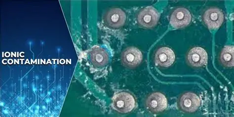
PCB contamination refers to the presence of ionic or non-ionic residues on board surfaces or within vias and under components. Ionic contamination arises primarily from flux residues, plating chemistries, and handling processes that leave soluble salts behind. These residues become mobile when moisture is present, enabling current leakage and dendritic growth between conductors. Non-ionic contaminants such as oils or particulates can trap moisture and exacerbate localized corrosion. In high-reliability sectors, unchecked contamination directly reduces mean time between failures and increases warranty returns. Engineers therefore treat cleanliness verification as an integral part of design validation rather than an afterthought.
Technical Principles and Mechanisms of PCB Corrosion
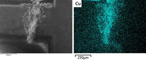
Ionic residues lower the surface insulation resistance by forming conductive paths when humidity exceeds the critical threshold for deliquescence. Under applied voltage, these paths support electrochemical migration, where metal ions from one conductor deposit onto an adjacent conductor, eventually creating shorts. Corrosion proceeds through anodic dissolution at one site and cathodic reduction at another, accelerated by the presence of halides or organic acids from flux. Temperature cycling further concentrates residues at interfaces, intensifying stress on solder joints and traces. The process follows established electrochemical kinetics described in industry test methods, where even parts-per-million levels of chloride can initiate failures within hundreds of hours under bias. Structured testing quantifies these risks before boards enter service.
Cleanliness Testing Methods and Industry Standards
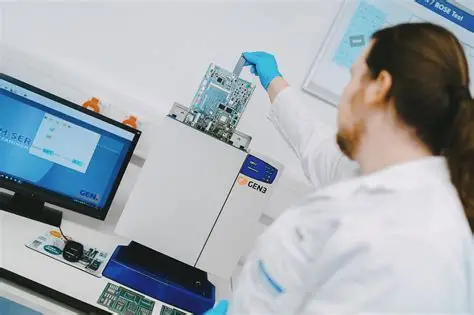
Cleanliness testing quantifies ionic contamination through extraction and measurement techniques that extract soluble residues into a known volume of solution. Resistivity of solvent extract testing provides a rapid indication of total ionic content, while ion chromatography offers species-specific data on chloride, bromide, and sulfate levels. Engineers select methods based on the required sensitivity and the board complexity. Reference to IPC-TM-650 ensures consistent procedures across laboratories and suppliers. These measurements establish pass-fail criteria tied directly to expected operating environments and voltage gradients. Consistent application of such protocols reduces variability in production and supports statistical process control.
Related Reading: A Deep Dive into IPC TM 650 Method 2.3.25: ROSE Testing for PCB Cleanliness
Practical Solutions and Best Practices for Engineers
Design teams incorporate cleanliness requirements into stack-up and layout rules by specifying minimum spacing that accounts for expected residue levels. Manufacturing partners implement controlled cleaning sequences after soldering, followed by verification sampling at defined intervals. Engineers review test data trends to adjust process parameters such as reflow profiles or cleaning solution concentrations before defects accumulate. When ionic levels approach specification limits, root-cause analysis focuses on flux selection, rinse effectiveness, and handling protocols. Documentation of test results alongside board serial numbers enables traceability and supports continuous improvement programs. These steps collectively enhance PCB reliability without introducing unnecessary process complexity.
Related Reading: PCB Contamination Challenges and Precision Cleaning Solutions
Troubleshooting Insights for Persistent Contamination Issues
When boards exhibit intermittent leakage or corrosion after deployment, engineers first correlate failure locations with historical cleanliness data from the same production lot. High-magnification inspection often reveals residue accumulation in high-density areas or under low-standoff components. Adjusting the extraction volume or temperature during re-testing can isolate whether the issue stems from surface or entrapped residues. Collaboration between design and process teams then evaluates alternative flux formulations or additional bake-out steps prior to conformal coating. Systematic logging of these investigations builds institutional knowledge that prevents recurrence in subsequent designs.
Conclusion
PCB contamination testing provides the quantitative foundation needed to prevent corrosion and maintain long-term reliability. By integrating extraction-based measurements with established process controls, engineers ensure that ionic residues remain below thresholds that trigger electrochemical degradation. The resulting boards exhibit stable insulation resistance and reduced susceptibility to dendritic growth across varied operating conditions. Consistent application of these practices throughout the product lifecycle translates directly into higher field performance and lower total cost of ownership.
FAQs
Q1: What is the primary purpose of PCB contamination testing?
A1: PCB contamination testing measures ionic residues left on board surfaces after fabrication and assembly. The data confirms that residue levels will not initiate corrosion or leakage under expected humidity and voltage conditions. Engineers use the results to validate cleaning processes and support long-term PCB reliability targets.
Q2: How does ionic contamination contribute to PCB corrosion?
A2: Ionic contamination supplies mobile ions that lower surface insulation resistance when moisture is present. These ions enable electrochemical migration and anodic dissolution, forming conductive dendrites between traces. Regular cleanliness testing identifies elevated ion levels before they accelerate PCB corrosion in service.
Q3: Which industry standards guide PCB cleanliness testing procedures?
A3: Procedures follow methods outlined in IPC-TM-650 for consistent extraction and measurement. Additional guidance appears in related IPC documents that define acceptance limits for different product classes. Adherence to these standards ensures repeatable results across suppliers and supports PCB reliability qualification.
Q4: Why should electrical engineers include cleanliness testing in design reviews?
A4: Including cleanliness testing early reveals process risks that layout rules alone cannot address. Engineers can then specify appropriate spacing, component selection, and cleaning requirements that protect against corrosion. This proactive step improves overall PCB reliability and reduces field failures.





