ALLPCB


Introduction
In PCB assembly lines, achieving high yield and reliability demands precise detection of defects that optical methods cannot reveal. Automated X-Ray Inspection, or AXI, emerges as a critical technology by providing non-destructive imaging of hidden solder joints and internal structures. This process automates quality control post-reflow soldering, targeting components like BGAs and QFNs where voids or misalignments compromise performance. Electric engineers appreciate AXI for its ability to integrate seamlessly into high-volume production, reducing false calls and manual intervention. By leveraging X-ray penetration, AXI ensures compliance with soldering standards while maximizing throughput. As assembly complexity grows, understanding AXI system advantages becomes essential for optimizing efficiency.
What Is AXI and Why It Matters in PCB Assembly
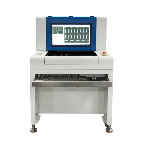
AXI stands for Automated X-Ray Inspection, a method that uses X-rays to generate images of PCB internals without disassembly. Unlike AOI, which relies on visible light for surface checks, AXI penetrates components to visualize solder joints beneath packages. This capability detects issues such as insufficient solder volume, bridging, or head-in-pillow defects that evade traditional inspections. In modern electronics, where bottom-terminated components dominate, AXI matters because it safeguards signal integrity and thermal performance. Engineers rely on it to verify assembly quality in real-time, preventing field failures in applications from consumer devices to aerospace. The automated X-Ray inspection process thus elevates overall line efficiency by minimizing rework.
Core Technical Principles of AXI
AXI operates on the principle of X-ray attenuation, where rays pass through the PCB and vary in intensity based on material density. Detectors capture these variations to form grayscale images, highlighting differences between solder, copper, and substrates. Modern systems employ 2D laminography or 3D computed tomography for layered views, resolving overlaps in dense assemblies. Software algorithms then analyze images against programmed thresholds, classifying defects automatically. Radiation safety features, like collimators, ensure operator protection during continuous operation. This foundation enables precise quantification of joint quality, aligning with criteria in IPC-A-610J for electronic assemblies.
Key AXI System Advantages for Electric Engineers
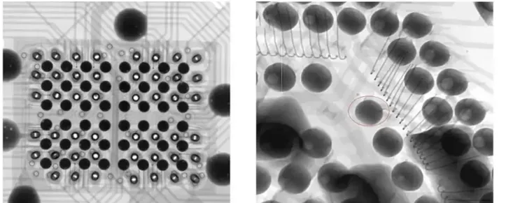
One primary AXI system advantage lies in its non-contact, high-speed scanning, processing hundreds of joints per minute without physical probing. Automation eliminates human error, delivering consistent results across shifts and operators. It excels at identifying volumetric defects like voids exceeding acceptable limits, which optical systems miss entirely. Inline AXI configurations allow immediate feedback post-reflow, halting defective lots early to cut scrap rates. Compared to manual X-ray, automation scales for high-mix production, adapting recipes per board type. These benefits compound in troubleshooting scenarios, where root cause analysis traces reflow profiles or paste issues swiftly.
The Automated X-Ray Inspection Process Step-by-Step
The automated X-Ray inspection process begins with board loading onto the conveyor, aligning fiducials for precise positioning. The X-ray source activates, emitting a controlled beam while the detector records multiple angles for reconstruction. Image acquisition takes seconds per region of interest, focusing on critical areas like BGAs. AI-driven software compares captures to golden references, flagging anomalies based on shape, size, and density. Results integrate with manufacturing execution systems for traceability. Operators review only flagged boards, streamlining the workflow.
AXI Programming: Essential Techniques for Optimal Performance
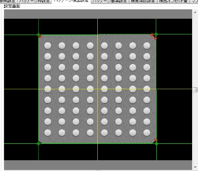
AXI programming starts with defining inspection zones via CAD data or manual teaching, specifying components and joint types. Engineers upload golden samples, good and bad, to train defect classifiers on voids or cracks. Thresholds set tolerances for fillet height or ball offset, calibrated to production variability. Recipe optimization involves false positive reduction through noise filtering and multi-angle validation. Regular updates account for process drifts, ensuring reliability. Troubleshooting poor programming often reveals mismatched references, resolved by re-teaching with current assembly data.
Implementing Inline AXI in Production Lines
Inline AXI positions post-reflow, inspecting full panels before separation to catch systemic issues. Conveyor speed matching maintains takt time, with dual-lane options for redundancy. Integration requires stable power and vibration isolation for image clarity. Benefits include real-time yield monitoring, triggering reflow adjustments proactively. Common pitfalls like beam hardening from thick boards demand oblique-angle programming. Electric engineers value this setup for its traceability, linking defects to upstream SPI or AOI data.
Integrating AXI with AOI for Comprehensive Coverage
Integrating AXI with AOI creates a hybrid inspection strategy, where AOI handles visible pre- and post-print defects rapidly. AOI flags potential issues, directing AXI to scrutinize hidden joints only, optimizing throughput. Data sharing via common protocols synchronizes results, reducing escape rates. This tandem verifies solder joint criteria per J-STD-001J requirements, covering both external and internal quality. Troubleshooting integration snags involves aligning fiducials and timing gates. The result is maximized efficiency, with AOI's speed complementing AXI's depth.
Best Practices and Troubleshooting for AXI Systems
Establish daily calibration using phantoms to verify resolution and contrast before runs. Maintain clean detectors and sources to prevent artifacts mimicking defects. Program conservatively initially, tightening thresholds after yield stabilization. For troubleshooting, log image archives to correlate failures with oven profiles or stencil wear. Avoid over-reliance on automation by periodic manual audits. Adhering to IPC-7095 guidelines for BGA inspection enhances programming accuracy.
In high-density boards, tilt artifacts signal misalignment, fixed by fiducial re-teaching. Excessive false calls often stem from recipe offsets, addressed by batch re-optimization. Radiation exposure monitoring ensures compliance with safety norms. These practices sustain AXI reliability across production scales.
Conclusion
AXI transforms PCB assembly inspection by automating detection of hidden defects, delivering AXI system advantages like speed and precision. From programming recipes to inline deployment and AOI integration, it empowers electric engineers to troubleshoot proactively. The automated X-Ray inspection process aligns with industry standards, ensuring robust assemblies. Implementing these strategies maximizes efficiency, reduces costs, and boosts quality. As production demands evolve, AXI remains indispensable for reliable electronics manufacturing.
FAQs
Q1: What are the main AXI system advantages in PCB assembly?
A1: AXI system advantages include non-destructive imaging of hidden solder joints, high automation for consistent results, and inline capability for real-time feedback. It detects volumetric defects like voids in BGAs that AOI misses, reducing rework and improving yield. Electric engineers benefit from quantifiable data for process optimization, aligning with standards like IPC-A-610J. Overall, it scales efficiently for high-volume lines without manual intervention.
Q2: How does the automated X-Ray inspection process work in practice?
A2: The automated X-Ray inspection process involves board alignment, X-ray emission, image capture via detectors, and software analysis against references. It generates 2D or 3D views to identify defects like bridging or insufficient solder. Inline systems process boards continuously, flagging issues for review. Troubleshooting focuses on calibration to maintain accuracy. This ensures comprehensive post-reflow quality control.
Q3: What is involved in AXI programming for custom boards?
A3: AXI programming requires defining zones from CAD, teaching good/bad samples, and setting defect thresholds for shape and density. Optimization minimizes false positives through multi-view validation. Updates adapt to process changes, crucial for high-mix production. Engineers troubleshoot by reviewing logs and re-calibrating. Effective programming enhances inline AXI performance and integrates seamlessly with AOI data.
Q4: How does integrating AXI with AOI improve efficiency?
A4: Integrating AXI with AOI leverages AOI for fast surface checks and AXI for hidden joints, creating full coverage without bottlenecks. Shared data enables targeted inspections, cutting overall time. It verifies compliance with J-STD-001J soldering criteria efficiently. Troubleshooting involves protocol alignment for smooth flow. This hybrid boosts yield in complex assemblies.
References
IPC-A-610J — Acceptability of Electronic Assemblies. IPC, 2024
IPC J-STD-001J — Requirements for Soldered Electrical and Electronic Assemblies. IPC, 2024