 ALLPCB


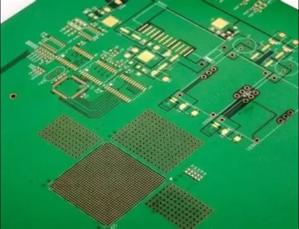
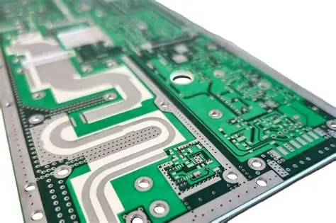
High-speed printed circuit boards demand precise control over electrical characteristics to maintain reliable data transmission. Impedance testing plays a central role in verifying that signal paths behave as intended, preventing reflections and distortions that can degrade performance. Engineers rely on controlled impedance designs to ensure consistent signal integrity across complex multilayer boards. Without proper verification, even minor deviations in trace geometry or material properties can lead to timing errors or data loss in applications such as telecommunications and computing systems.
What Is Controlled Impedance and Why It Matters
Controlled impedance refers to the deliberate design of transmission lines on a printed circuit board so that their characteristic impedance matches a specified value, typically 50 ohms or 100 ohms for differential pairs. This matching minimizes signal reflections and preserves waveform integrity at high frequencies. In high-speed PCBs, even small mismatches can cause electromagnetic interference and reduce overall system reliability. Manufacturers therefore incorporate impedance testing as a standard quality step to confirm that fabricated boards meet design targets. The practice supports compliance with established performance specifications and helps engineers predict real-world behavior before assembly.
Technical Principles of Impedance Measurement Techniques
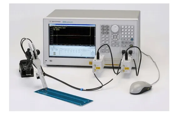
Impedance arises from the interaction of inductance, capacitance, and resistance along a conductor, governed by the physical dimensions of the trace, the dielectric constant of the substrate, and the spacing to reference planes. Accurate modeling begins with calculating the impedance using formulas that account for trace width, thickness, and dielectric height. Deviations during fabrication, such as etching variations or lamination inconsistencies, alter these parameters and shift the actual impedance away from the target. Time-domain reflectometry, commonly known as TDR testing, sends a fast-rising pulse down the line and analyzes the reflected waveform to locate impedance discontinuities. Frequency-domain methods complement TDR by measuring scattering parameters across a bandwidth relevant to the operating speed. Together these impedance measurement techniques provide both spatial resolution and broadband characterization essential for validating high-speed designs.
Related Reading: PCB Impedance Testing: Why It Matters for Signal Integrity
Practical Solutions and Best Practices for PCB Impedance Testing
Engineers begin by specifying target impedance values and tolerance bands during the schematic and layout phases, then communicate these requirements clearly to fabrication teams. Design rules must incorporate appropriate trace geometries and stack-up configurations that achieve the desired impedance while respecting manufacturing capabilities. During production, test coupons fabricated alongside the main board allow non-destructive verification using TDR or vector network analyzers. Regular calibration of test equipment ensures measurement accuracy, and statistical process control tracks impedance variation across production lots. When discrepancies appear, root-cause analysis examines etch factors, copper thickness, and dielectric thickness to guide corrective actions. These steps collectively reduce the risk of signal integrity failures in the final assembly.
According to IPC-6012E, qualification and performance requirements for rigid printed boards include verification of controlled impedance structures as part of acceptance testing.
Related Reading: Decoding Impedance Testing: A Comprehensive Guide for PCB Design
Troubleshooting Impedance Issues in High-Speed Designs
Common impedance deviations stem from inconsistent dielectric thickness or trace width variations introduced during etching. Engineers troubleshoot by comparing measured TDR profiles against simulated waveforms to isolate the location and magnitude of mismatches. Adjusting the stack-up or modifying trace widths in subsequent revisions often restores the target impedance without redesigning the entire board. In cases where material properties contribute to drift, evaluating alternative substrates with tighter dielectric tolerances provides a practical path forward. Systematic documentation of test results supports continuous improvement and helps teams refine design guidelines for future projects.
Conclusion
Mastering impedance testing ensures that high-speed PCBs deliver the signal integrity required by modern electronic systems. By combining accurate modeling, rigorous measurement techniques, and adherence to industry specifications, engineers can identify and correct deviations early in the manufacturing cycle. Consistent application of these practices reduces costly rework and enhances product reliability across demanding applications.
FAQs
Q1: What is pcb impedance testing and how does it support controlled impedance?
A1: Pcb impedance testing measures the actual characteristic impedance of transmission lines on a fabricated board and compares the results to design targets. This verification confirms that trace geometry and dielectric properties produce the intended controlled impedance values. Engineers use the data to validate manufacturing processes and maintain signal integrity in high-frequency circuits.
Q2: How does TDR testing contribute to signal integrity in high-speed PCBs?
A2: TDR testing launches a fast pulse along a trace and records reflections caused by impedance changes, revealing the precise location and severity of discontinuities. The resulting waveform allows engineers to quantify deviations from the target impedance and correlate them with physical features on the board. This method provides actionable information for correcting layout or process issues before they affect overall signal integrity.
Q3: What are the main impedance measurement techniques used during PCB production?
A3: Common impedance measurement techniques include time-domain reflectometry for spatial mapping of impedance along a trace and frequency-domain analysis for broadband characterization. Both approaches rely on calibrated test equipment and standardized coupons to ensure repeatable results. Together they enable comprehensive validation of controlled impedance designs against performance requirements.
Q4: Why is controlled impedance verification important for electrical engineers working on high-speed designs?
A4: Controlled impedance verification confirms that fabricated boards match the electrical parameters assumed during simulation and layout. Without this step, reflections and distortions can compromise timing margins and increase bit-error rates in high-speed applications. Regular testing therefore forms an essential part of quality assurance for reliable system performance.
References
IPC-6012E — Qualification and Performance Specification for Rigid Printed Boards. IPC, 2017
IPC-A-600K — Acceptability of Printed Boards. IPC, 2020


