 ALLPCB


In a world increasingly focused on sustainability, how can the electronics industry reduce its environmental impact? One key area of focus is sustainable PCB packaging, which plays a vital role in achieving a circular economy. By prioritizing circular economy PCB packaging, reducing carbon footprint in PCB packaging, and embracing concepts like life cycle assessment and cradle to cradle design, manufacturers can minimize waste and promote eco-friendly practices. In this blog, we’ll dive deep into how sustainable PCB disposal and innovative packaging solutions can help build a greener future for the electronics industry.
Why Sustainable PCB Packaging Matters in a Circular Economy
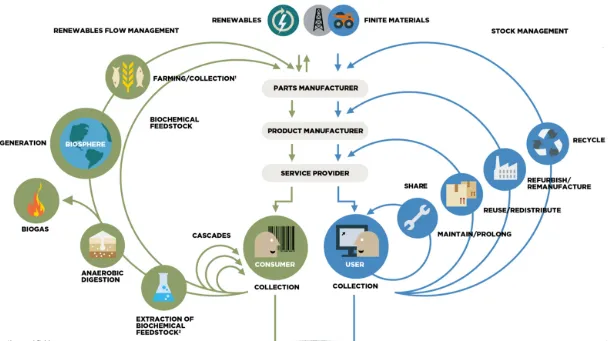
The concept of a circular economy is simple: instead of the traditional "take-make-waste" model, we aim to reuse, recycle, and repurpose materials to keep them in circulation. For printed circuit boards (PCBs), which are at the heart of nearly every electronic device, packaging plays a critical role in this process. PCB packaging not only protects components during transport but also contributes significantly to the overall environmental footprint of electronics manufacturing.
Traditional PCB packaging often relies on single-use plastics and non-recyclable materials, which end up in landfills or as pollution. By focusing on circular economy PCB packaging, the industry can reduce waste, lower carbon emissions, and conserve valuable resources. Sustainable packaging solutions also align with growing regulatory demands and consumer expectations for greener practices.
Reducing Carbon Footprint in PCB Packaging: Key Strategies
Reducing the carbon footprint of PCB packaging is a critical step toward sustainability. The production, transportation, and disposal of packaging materials all contribute to greenhouse gas emissions. Here are some actionable strategies to minimize this impact:
- Use Recyclable Materials: Opt for packaging made from recycled cardboard, paper, or bioplastics. These materials have a lower carbon footprint compared to virgin plastics, which require significant energy to produce.
- Minimize Packaging Size: Design compact packaging that uses less material without compromising protection. For example, custom-fit cardboard inserts can reduce the need for excess filler materials by up to 30%, cutting down on both waste and shipping emissions.
- Optimize Transportation: Lightweight packaging reduces fuel consumption during shipping. Switching to eco-friendly logistics partners who use electric or hybrid vehicles can further lower emissions by an estimated 20-40%, depending on the fleet.
- Adopt Renewable Energy in Production: Packaging manufacturers can reduce emissions by powering facilities with solar or wind energy, cutting down the carbon footprint of production by as much as 50% in some cases.
By integrating these practices, companies can make significant strides in reducing carbon footprint in PCB packaging, contributing to a more sustainable supply chain.
Life Cycle Assessment for PCB Packaging: Understanding the Full Impact
A life cycle assessment (LCA) for PCB packaging is a powerful tool to evaluate the environmental impact of a product from cradle to grave. This method analyzes every stage of the packaging’s life, including raw material extraction, production, use, and disposal. Conducting an LCA helps identify areas where improvements can be made to reduce environmental harm.
For example, an LCA might reveal that the energy-intensive production of plastic packaging contributes 60% of its total carbon emissions. Armed with this data, manufacturers can switch to materials like recycled paper, which may cut emissions by half during production. Additionally, an LCA can highlight the benefits of reusable packaging systems, showing how they reduce waste by up to 70% over single-use options.
Implementing life cycle assessment for PCB packaging ensures that decisions are based on hard data, leading to more sustainable outcomes. It also helps companies comply with regulations and build trust with environmentally conscious customers who value transparency.
Cradle to Cradle PCB Packaging: Designing for Reuse and Recycling
The cradle to cradle (C2C) design philosophy takes sustainability a step further by ensuring that products are designed with their entire life cycle in mind. For PCB packaging, this means creating materials that can be reused or recycled indefinitely without losing value. Unlike the traditional "cradle to grave" model, cradle to cradle PCB packaging focuses on eliminating waste altogether.
One example of C2C in action is the use of biodegradable packaging materials that break down naturally without releasing toxic substances. Another approach is modular packaging designs that allow components to be reused for multiple shipments. For instance, a reusable PCB tray system could reduce packaging waste by 80% over five cycles of use, based on industry estimates.
Additionally, C2C encourages the use of non-toxic adhesives and coatings in packaging to ensure that materials can be safely recycled. By designing for disassembly, manufacturers make it easier to separate components at the end of their life, promoting a truly circular economy.
Sustainable PCB Disposal: Closing the Loop
Disposal is often the most overlooked aspect of PCB packaging, yet it’s a crucial part of achieving a circular economy. Sustainable PCB disposal involves ensuring that packaging materials are either recycled, composted, or repurposed rather than sent to landfills. Here’s how this can be achieved:
- Recycling Programs: Establish take-back programs where used packaging is returned to the manufacturer for recycling. This can recover up to 90% of materials like cardboard and certain plastics for reuse.
- Compostable Materials: Use packaging made from compostable materials, such as plant-based bioplastics, which decompose naturally within 6-12 months under the right conditions.
- Education and Labeling: Clearly label packaging with disposal instructions to guide end-users on how to recycle or compost materials. Studies show that proper labeling can increase recycling rates by 25%.
- Partnerships with Waste Management: Collaborate with specialized waste management companies to handle packaging materials at the end of their life, ensuring proper processing and minimal environmental impact.
Sustainable PCB disposal not only reduces landfill waste but also conserves resources by reintroducing materials into the production cycle. It’s a vital step in closing the loop of a circular economy.
Challenges in Implementing Sustainable PCB Packaging
While the benefits of sustainable PCB packaging are clear, there are challenges to overcome. Cost is often a significant barrier, as eco-friendly materials like bioplastics can be 20-30% more expensive than traditional plastics. Additionally, the infrastructure for recycling or composting may not be widely available in all regions, limiting the effectiveness of sustainable disposal practices.
Another challenge is balancing sustainability with functionality. PCB packaging must protect delicate components from static, moisture, and physical damage. Finding eco-friendly materials that meet these strict requirements can be difficult, though innovations like biodegradable anti-static films are beginning to bridge this gap.
Finally, regulatory differences across countries can complicate global supply chains. What’s considered recyclable in one region might be treated as waste in another. Harmonizing standards and investing in research for universal solutions will be key to overcoming these hurdles.
Innovations Driving Sustainable PCB Packaging
The good news is that technology and innovation are paving the way for more sustainable PCB packaging. Here are a few exciting developments:
- Bio-Based Materials: New plant-based packaging materials are being developed that offer the same protective qualities as plastics but with a fraction of the environmental impact. Some of these materials reduce carbon emissions by up to 60% during production.
- Smart Packaging: Incorporating sensors into packaging can extend its life by monitoring conditions like humidity or temperature, ensuring PCBs remain protected during multiple uses.
- 3D-Printed Packaging: Additive manufacturing allows for custom packaging with minimal material waste. This can reduce excess material usage by 40% compared to traditional methods.
These innovations show that sustainability and performance can go hand in hand, offering hope for a carbon-neutral future in PCB packaging.
How Manufacturers Can Transition to Circular Economy Practices
Transitioning to circular economy PCB packaging requires a strategic approach. Manufacturers can start by conducting a baseline assessment of their current packaging processes to identify high-impact areas for improvement. Partnering with suppliers who prioritize sustainability can ensure a steady supply of eco-friendly materials.
Investing in employee training is also essential. Educating staff on sustainable practices, from design to disposal, ensures that everyone is aligned with the company’s green goals. Finally, transparency with customers about sustainability efforts can build trust and loyalty, as more than 70% of consumers prefer to support environmentally responsible brands, according to recent surveys.
The Future of Sustainable PCB Packaging
The journey toward a carbon-neutral circuit is just beginning, but the momentum is undeniable. As regulations tighten and consumer demand for sustainability grows, the electronics industry must continue to innovate in circular economy PCB packaging. By focusing on reducing carbon footprint in PCB packaging, embracing life cycle assessment, adopting cradle to cradle principles, and prioritizing sustainable PCB disposal, manufacturers can lead the way in building a greener future.
At every step, from design to disposal, there are opportunities to make a difference. Sustainable PCB packaging isn’t just a trend—it’s a necessity for preserving our planet for future generations. With the right strategies and innovations, the industry can close the loop and achieve a truly circular economy.


