 ALLPCB


High-speed digital circuits operating at multi-gigabit data rates place stringent demands on printed circuit board performance. Signal degradation arises from losses, reflections, and crosstalk that distort waveforms and close eye diagrams. HDI PCB technology addresses these challenges by enabling finer conductor features, smaller vias, and more controlled stackups than conventional boards. Designers working on servers, networking equipment, and advanced computing platforms increasingly rely on HDI constructions to maintain signal integrity while achieving higher component density. The approach requires careful attention to materials, geometry, and layout practices that keep impedance consistent and minimize discontinuities.
What Is HDI PCB High-Speed Design and Why It Matters
HDI PCB high-speed design refers to the use of high-density interconnect techniques, such as microvias, sequential lamination, and fine-line routing, specifically optimized for circuits where edge rates and data rates push signal integrity limits. These boards feature track widths and spaces often below 75 micrometers, along with laser-drilled vias that reduce stub lengths compared with through-hole vias. The result is shorter signal paths and lower parasitic inductance and capacitance. In high-speed applications, even small impedance variations or excessive via stubs can produce reflections that degrade rise times and increase jitter. Industry standards such as IPC-2221B guide the design rules that keep these effects within acceptable bounds for reliable operation at multi-gigahertz frequencies.
Technical Principles of Signal Degradation in HDI Boards
Signal degradation in high-speed digital circuits stems primarily from conductor loss, dielectric loss, and reflections caused by impedance mismatches. At frequencies above a few gigahertz, skin effect increases effective resistance in copper traces, while the dissipation factor of the dielectric converts energy into heat. Microvias in HDI constructions shorten the vertical transitions that would otherwise act as stubs and create resonant reflections. Crosstalk between adjacent traces also rises with tighter spacing, although the controlled geometries possible in HDI help maintain adequate spacing-to-height ratios. Eye diagram closure occurs when deterministic jitter from these mechanisms accumulates, reducing the timing margin available for receivers. Maintaining consistent characteristic impedance along the entire path, including through vias and connectors, is therefore essential.
Impedance matching in HDI PCB high-speed design relies on precise control of trace width, dielectric thickness, and copper thickness. Differential pairs require matched lengths and symmetric return paths to preserve common-mode rejection. Any change in reference plane or via transition alters the local impedance and launches reflections that appear as ringing or overshoot. Low-loss laminate materials with stable dielectric constants across frequency reduce both attenuation and phase distortion. Thermal expansion differences between layers can also induce warpage that subtly changes trace geometry after reflow, affecting impedance.
Practical Solutions and Best Practices
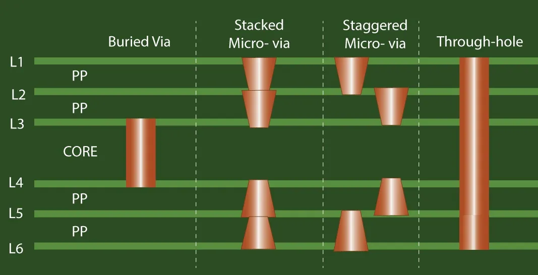
Designers begin by selecting a stackup that places signal layers adjacent to reference planes while keeping microvia depths shallow. Sequential lamination allows buried vias that eliminate stubs entirely for critical nets. Trace widths are calculated from the target impedance, typically 85 or 100 ohms for differential pairs, using the dielectric constant and thickness values provided by the laminate supplier. Length matching within a few mils for high-speed pairs prevents skew that converts differential signals into common-mode noise. Via pads are sized and spaced to avoid excessive capacitance, and back-drilling or filled vias further reduce discontinuities where through vias remain necessary.
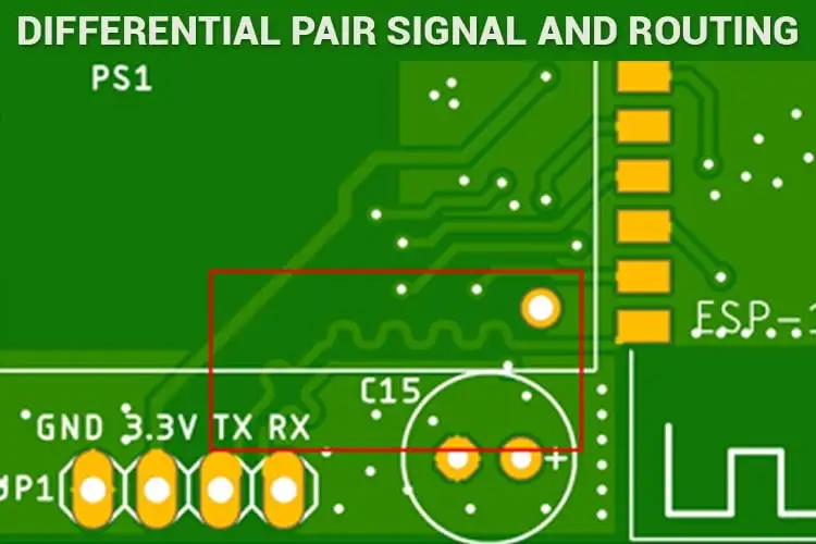
Routing practices emphasize smooth transitions and avoidance of 90-degree bends that create impedance steps. Differential pairs are routed with consistent spacing and minimal layer changes. When layer transitions occur, ground vias placed close to signal vias maintain return-path continuity. Power distribution networks are designed with low inductance planes and sufficient decoupling to prevent supply noise from modulating signal levels. Simulation of the full channel, including package and connector models, verifies that eye height and jitter remain within specifications before fabrication.
Material selection focuses on laminates with low dissipation factor and stable dielectric properties up to the operating frequency. Copper foil roughness is minimized on high-speed layers to reduce conductor loss. Fabrication tolerances for trace width and dielectric thickness are tightened beyond standard requirements to keep impedance variation within plus or minus five percent. Post-lamination testing confirms that warpage stays within limits that would otherwise affect connector mating or via reliability.
Troubleshooting Common Signal Integrity Issues
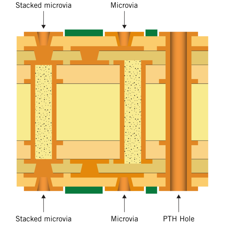
When eye diagrams show excessive jitter or closure, the first step is to measure actual impedance along critical nets using time-domain reflectometry. Deviations often trace to via stubs, inconsistent dielectric thickness, or reference plane discontinuities. Adjusting the stackup to move sensitive signals to layers with better plane adjacency or converting to blind microvias frequently restores margin. Length tuning and serpentine routing correct skew, while adding stitching vias reduces crosstalk. In cases of unexpected attenuation, laminate moisture absorption or surface roughness may be contributing factors that require material or process adjustments.
Related Reading: HDI PCB Design for High Speed Applications: Overcoming Density Challenges
Conclusion
HDI PCB high-speed design provides the geometric precision and via flexibility needed to keep signal degradation within acceptable limits at multi-gigabit rates. Consistent impedance control, minimized via stubs, and low-loss materials form the foundation of reliable performance. Structured stackup planning combined with careful routing and simulation ensures that eye diagrams remain open and jitter stays low. Adherence to established design standards supports repeatable manufacturing outcomes across production volumes.
FAQs
Q1: How does HDI PCB high-speed design improve signal integrity compared with standard boards?
A1: HDI constructions use microvias and finer features that shorten signal paths and reduce parasitic effects. This lowers reflections and crosstalk while allowing tighter impedance control. The result is cleaner eye diagrams and reduced jitter at high data rates.
Q2: What role does impedance matching play in HDI PCB signal integrity?
A2: Impedance matching prevents reflections that distort waveforms and close eye openings. In HDI boards, precise trace geometry and dielectric thickness maintain the target impedance through microvia transitions. Consistent matching preserves signal amplitude and timing margins.
Q3: How can designers minimize jitter in HDI PCB high-speed circuits?
A3: Jitter is reduced by eliminating via stubs, matching trace lengths, and maintaining continuous return paths. Low-loss materials and controlled copper roughness limit deterministic jitter sources. Full-channel simulation verifies performance before fabrication.
Q4: Why is material selection critical for HDI PCB high-speed design?
A4: Laminate dielectric constant and dissipation factor directly affect attenuation and phase velocity. Stable, low-loss materials preserve signal amplitude and edge rates across the operating frequency range. Consistent material properties also support tight impedance tolerances during manufacturing.





