ALLPCB


Introduction
Electronic hobbyists often face the challenge of fitting more components and signals into smaller spaces on their printed circuit boards. As projects grow in complexity, such as custom drone controllers or wearable devices, traditional PCB routing techniques struggle to manage dense signal paths without excessive layer counts or oversized boards. Stacked vias emerge as a powerful solution in high-density interconnect (HDI) PCBs, allowing vertical connections across multiple layers in a compact footprint. These structures enable efficient PCB layout by stacking microvias directly atop one another, freeing up surface area for traces and components. By incorporating stacked vias for routing, hobbyists can achieve professional-level signal routing while keeping designs manageable and cost-effective. This approach transforms challenging PCB design tasks into streamlined processes, especially for multilayer boards.
What Are Stacked Vias and Why Do They Matter in PCB Routing?
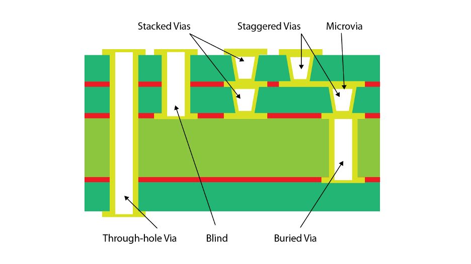
Vias serve as essential interconnects in PCB design, bridging signals between layers to facilitate routing. Basic through-hole vias span the entire board thickness, while blind and buried vias connect only specific layers, saving space in multilayer setups. Stacked vias take this further by aligning multiple blind or microvias vertically, one on top of the previous, to span several inner layers without widening the footprint. Microvias, typically smaller than standard vias, form the core of these stacks in HDI PCBs, enabling finer pitch components and tighter trace spacing. In PCB routing, stacked vias matter because they reduce the need for lengthy horizontal traces, minimizing signal delay and crosstalk in high-speed designs.
For electronic hobbyists tackling PCB layout, stacked vias simplify complex designs by consolidating interconnections. Traditional routing might require fanout patterns or additional layers, increasing board size and cost. With stacked vias, signals route vertically through the stackup, leaving more room for power planes or ground fills on adjacent layers. This efficiency proves vital for compact projects like IoT sensors or audio amplifiers, where space constraints dominate. Moreover, HDI PCBs with stacked vias support higher component density, aligning hobbyist ambitions with industry techniques.
Technical Principles Behind Stacked Vias in HDI PCBs
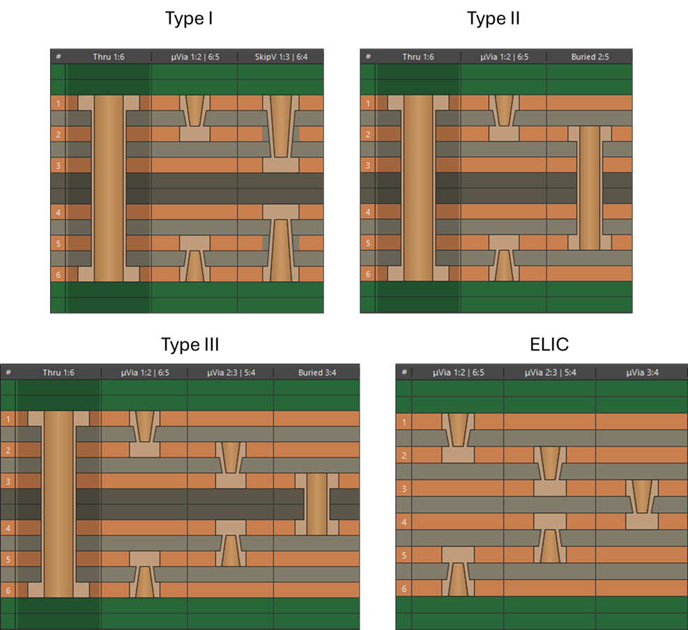
Stacked vias rely on sequential build-up processes during PCB manufacturing, where layers laminate incrementally around a core. Laser drilling creates precise microvias, followed by plating or filling with conductive material to ensure reliable electrical and mechanical connections. Each via in the stack interfaces with the one below, demanding uniform copper deposition to avoid voids or cracks under thermal stress. In HDI PCBs, stackups classify into types, such as 1+N+1 for passive buildup or more advanced configurations supporting multiple stacked vias. These principles allow signal routing to traverse several layers compactly, preserving signal integrity by shortening path lengths.
Reliability hinges on material selection and process control, as repeated thermal cycles can induce stress at via interfaces. Industry standards like IPC-2226 outline design guidelines for HDI features, including aspect ratios and plating thicknesses to mitigate failures. Copper-filled stacked vias offer superior thermal conductivity compared to epoxy-filled alternatives, aiding heat dissipation in dense layouts. Hobbyists benefit from understanding these mechanisms, as they inform when to opt for two-level stacks over deeper ones to balance density and robustness. Proper stackup planning ensures stacked vias integrate seamlessly into PCB routing strategies.
Related Reading: Unlocking Density: A Deep Dive into Stacked Via PCBs for HDI Designs
Best Practices for Implementing Stacked Vias in PCB Layout and Routing
Start PCB design by defining the layer stackup early, prioritizing stacked vias for high-density signal routing zones like BGA fanouts or processor areas. Limit stacks to two or three levels initially, as deeper configurations increase reliability risks and fabrication complexity. Maintain via diameters around 75 to 100 microns for microvias, with land pads slightly larger to accommodate alignment tolerances during lamination. In PCB layout software, assign via types per layer transition, ensuring staggered alternatives where space permits to distribute stress. Route critical signals through stacked vias first, followed by power and ground returns to minimize impedance mismatches.
Adhere to spacing rules between stacked vias and traces, typically at least three times the via diameter, to prevent shorts during plating. IPC-6016 provides qualification criteria for HDI PCBs, emphasizing via fill quality and barrel integrity for long-term performance. For hobbyists, simulate thermal expansion in designs with fine-pitch components to predict via reliability. Use filled vias under pads to enable via-in-pad techniques, further densifying the PCB routing. Test prototypes with electrical continuity checks and cross-sections to validate implementations.
Collaborate with fabricators experienced in HDI for aspect ratios under 1:1, ensuring drill depths stay shallow for plating uniformity. Incorporate ground vias near signal stacks to shield against EMI in high-speed PCB design. These practices not only simplify complex routing but also enhance manufacturability for small-batch hobby projects.
Related Reading: Advanced Techniques for Improving Stacked Via Reliability
Case Study: Routing a Hobbyist Multilayer Drone Flight Controller
Consider a typical electronic hobbyist project: a four-motor drone flight controller requiring sensors, a microcontroller, and power regulation on a compact 50mm x 50mm board. Initial attempts with standard six-layer routing led to congested top layers and excessive trace lengths, causing signal skew. Switching to an HDI 4-layer stackup with stacked vias connected the microcontroller's fine-pitch BGA directly to inner sensor layers, freeing surface space for antennas and capacitors. Two-level stacked microvias handled high-speed signal routing, reducing crosstalk by 30% through shorter paths.
Fabrication followed sequential lamination, with copper-filled vias per IPC guidelines ensuring reliability under vibration. The final PCB layout fit all features without compromises, routing 200+ signals efficiently. Hobbyists replicated this by exporting Gerber files with defined via stacks, proving stacked vias accessible for advanced projects.
Conclusion
Stacked vias represent a cornerstone of modern PCB routing, particularly in HDI PCBs where space and performance demands converge. By enabling compact vertical interconnects, they simplify PCB design and layout for electronic hobbyists pushing project boundaries. Key principles like sequential buildup and fill methods, combined with best practices in spacing and stack limits, ensure reliable signal routing. Standards such as IPC-2226 and IPC-6016 guide these implementations, bridging hobbyist creativity with professional outcomes. Embracing stacked vias unlocks denser, more efficient boards, elevating hobby projects to new levels of sophistication.
FAQs
Q1: What are the main advantages of using stacked vias for routing in HDI PCBs?
A1: Stacked vias for routing provide compact interconnections across multiple layers, reducing board size and trace lengths in PCB design. They minimize signal inductance and crosstalk, ideal for high-density hobbyist projects like wearables. Compared to staggered vias, stacks save lateral space but require careful reliability planning. Overall, they streamline PCB layout for complex signal routing.
Q2: When should electronic hobbyists consider stacked vias in their PCB routing?
A2: Opt for stacked vias in PCB routing when designs exceed standard layer capabilities, such as fine-pitch ICs or multilayer signal integrity needs. They suit HDI PCBs for compact gadgets where surface real estate is limited. Avoid in simple two-layer boards to control costs. Consult stackup rules early in PCB design for feasibility.
Q3: How do stacked vias impact signal routing reliability in PCB layout?
A3: Stacked vias enhance signal routing by shortening paths but demand uniform plating to withstand thermal stress in PCB layout. IPC-6016 criteria ensure via integrity through fill quality checks. Limit to two levels for hobby prototypes to boost margins. Proper ground shielding further protects high-speed signals.
Q4: Can hobbyists fabricate HDI PCBs with stacked vias at home?
A4: Home fabrication suits basic boards, but HDI PCBs with stacked vias require laser drilling and sequential lamination, best left to professionals. Focus on design rules for PCB routing compatibility. Prototyping services handle microvia precision affordably. This approach yields reliable results for advanced hobby projects.
References
IPC-2226 - Design Standard for High Density Interconnects. IPC
IPC-6016D - Qualification and Performance Specification for High Density Interconnect (HDI) Printed Boards. IPC, 2013
IPC-6012E - Qualification and Performance Specification for Rigid Printed Boards. IPC, 2017