 ALLPCB


Solder mask bridging occurs when the protective coating on a printed circuit board fails to maintain proper separation between conductive features. This condition allows solder to flow across unintended paths during assembly, creating electrical shorts. Engineers encounter this issue across high-density designs where component spacing continues to shrink. The problem directly affects yield rates and long-term reliability in electronic products.
What Is Solder Mask Bridging and Why It Matters
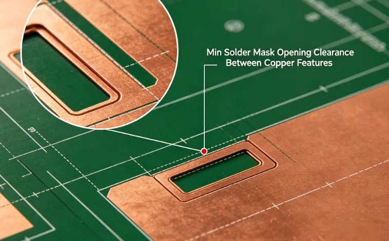
Solder mask bridging refers to the formation of unwanted conductive paths caused by incomplete or misplaced solder mask material. It differs from simple solder bridges because the mask itself contributes to the defect through slivers or insufficient clearance. In modern PCB layouts, trace widths and pad spacings often fall below 0.15 millimeters, increasing the risk of such defects. Industry standards such as IPC-A-600K define acceptable mask coverage and clearance requirements to prevent these issues.
The relevance of solder mask bridging extends beyond immediate manufacturing defects. It can lead to intermittent failures that surface only after thermal cycling or vibration exposure. Procurement teams and design engineers must address clearance rules early to avoid costly rework. Proper understanding of mask application limits helps maintain signal integrity in high-speed circuits.
Technical Principles and Mechanisms of Solder Mask Bridging
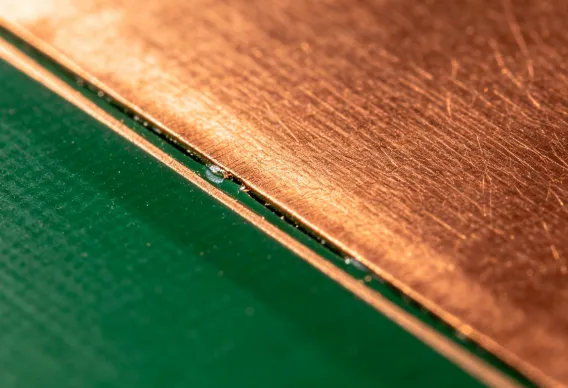
The primary mechanism involves solder mask slivers that remain between closely spaced copper features after development. These slivers form when mask material does not fully clear during the imaging and etching process. Surface tension during reflow then pulls molten solder along the sliver, completing an electrical connection. Factors such as mask thickness, exposure energy, and development chemistry influence sliver formation.
Another mechanism arises from insufficient solder mask clearance relative to copper pad or trace dimensions. When clearance falls below recommended values, mask misalignment during registration creates partial coverage over copper. This partial coverage allows solder paste to bridge during stencil printing or reflow. Thermal expansion differences between the mask and substrate can further exacerbate the problem during soldering.
Design rules must account for mask registration tolerances typically ranging from 0.05 to 0.075 millimeters. Failure to incorporate these tolerances results in bridging even when nominal clearances appear adequate. Structured review of artwork files against mask design guidelines reduces the occurrence of these defects.
Related Reading: Understanding Solder Mask Bridge in PCB Design
Practical Solutions and Best Practices for Prevention
Designers should apply minimum solder mask clearance values of 0.1 millimeters or greater between copper features, depending on board class and mask type. Increasing clearance provides margin for registration errors and improves mask adhesion. Software design rule checks can flag violations before artwork release.
During manufacturing, precise control of mask exposure and development parameters minimizes sliver formation. Post-development inspection verifies complete removal of mask material from intended openings. IPC-6012E outlines qualification requirements that include verification of mask clearance and coverage.
Assembly processes benefit from optimized stencil aperture designs that reduce excess solder volume near mask edges. Controlled reflow profiles limit the time solder remains molten, decreasing the chance of flow along any residual slivers. Regular process audits help maintain these controls across production lots.
Related Reading: The role of Solder Mask on preventing solder bridges
Troubleshooting Insights for Persistent Bridging Issues
When bridging persists after clearance adjustments, engineers examine mask thickness and material properties. Thicker masks can trap slivers more readily, while certain formulations offer improved resolution. Cross-section analysis of affected boards reveals whether the defect originates in mask application or subsequent handling.
Thermal and mechanical stress testing identifies latent bridges that may not appear during initial electrical testing. Boards that pass initial inspection yet fail after reflow simulation indicate marginal clearance or mask adhesion problems. Documentation of failure locations supports targeted corrective actions in the design or process flow.
Conclusion
Solder mask bridging remains a controllable defect when clearance rules and process controls receive proper attention. Early incorporation of adequate spacing in PCB layouts, combined with adherence to established industry standards, significantly reduces short-circuit risks. Consistent application of these practices supports higher yields and improved product reliability across electronic assemblies.
FAQs
Q1: What causes solder mask bridging in PCB manufacturing?
A1: Solder mask bridging primarily results from insufficient clearance between copper features or incomplete removal of mask material during development. These conditions allow solder to flow across unintended paths during reflow. Maintaining recommended clearance values and verifying mask resolution during fabrication prevents most occurrences.
Q2: How does solder mask clearance affect preventing solder bridges?
A2: Adequate solder mask clearance ensures the protective layer fully separates adjacent copper areas, blocking solder flow. Clearance values below process tolerances increase the likelihood of slivers or partial coverage. Designers incorporate registration allowances to maintain effective separation throughout assembly.
Q3: What role does solder mask slivers play in PCB short circuit causes?
A3: Solder mask slivers act as bridges that guide molten solder between closely spaced conductors. They form when mask material fails to clear completely from narrow gaps. Removing these slivers through optimized imaging and development steps directly reduces short-circuit defects.
Q4: How can engineers implement solder mask bridging prevention in design?
A4: Engineers apply design rule checks that enforce minimum clearance and account for mask registration tolerances. They also select mask materials and thicknesses compatible with the intended trace and pad geometries. Collaboration with fabrication teams confirms that layout rules align with actual process capabilities.
References
IPC-A-600K — Acceptability of Printed Boards. IPC, 2020
IPC-6012E — Qualification and Performance Specification for Rigid Printed Boards. IPC, 2017
J-STD-001H — Requirements for Soldered Electrical and Electronic Assemblies. IPC, 2020


