 ALLPCB


Introduction
In high-speed double-sided PCB design, signal integrity double-sided PCB performance hinges on precise impedance control. Double-sided PCBs, with conductive layers on both sides of the substrate, offer cost-effective solutions for many applications but pose unique challenges for maintaining consistent signal paths. As frequencies rise, mismatches in trace impedance lead to reflections, crosstalk, and waveform distortion, compromising data integrity. Engineers must prioritize controlled impedance double-sided PCB strategies to ensure reliable transmission. This article explores the principles, calculations, and best practices for double-sided PCB impedance matching, drawing on established engineering fundamentals. By mastering these elements, designers can optimize high-speed double-sided PCB design without escalating to multilayer boards.
What Is Impedance Control and Why It Matters in Double-Sided PCBs
Impedance control refers to designing and manufacturing PCB traces to exhibit a specific characteristic impedance, typically 50 ohms single-ended or 100 ohms differential. In double-sided PCBs, this involves configuring traces as microstrip lines, where the signal path runs over a reference plane on the opposite side. Without control, variations in trace geometry or material properties cause impedance discontinuities, leading to signal reflections that degrade eye diagrams and increase bit error rates. Signal integrity double-sided PCB issues become pronounced above 100 MHz, where transmission line effects dominate. Industry standards like IPC-2141A emphasize controlled impedance to support high-speed logic design. Ultimately, effective impedance matching prevents power loss and electromagnetic interference, enabling robust performance in compact designs.
The relevance intensifies in applications like USB 2.0, Ethernet, or clock distribution, where double-sided boards balance density and economy. Poor control amplifies noise coupling between layers, as the lack of embedded planes heightens sensitivity to routing decisions. Engineers benefit from understanding these dynamics to avoid redesign iterations.
Technical Principles of Impedance in Double-Sided PCBs
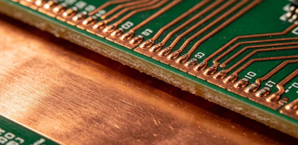
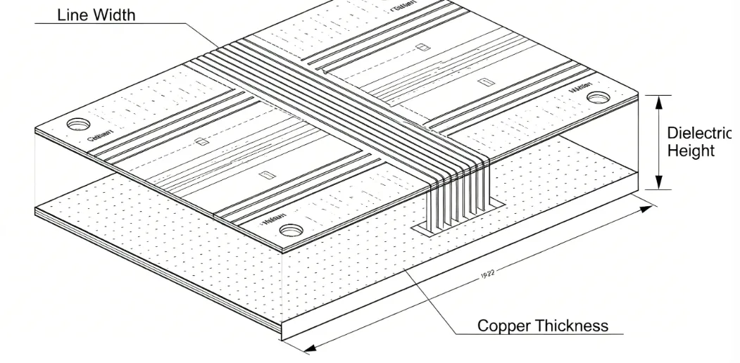
Characteristic impedance arises from the interplay of inductance and capacitance along a transmission line. For microstrip traces in double-sided PCBs, the signal conductor on one side couples to a ground plane on the other through the dielectric substrate. Key factors include trace width, copper thickness, substrate height, and dielectric constant (Er). Wider traces lower impedance by increasing capacitance, while thicker substrates raise it by reducing fringing fields. Air above the trace also contributes to effective Er, typically around 4.0-4.5 for FR-4 materials. These parameters define the wave propagation velocity and attenuation.
In double-sided configurations, the ground plane must be continuous and stitched with vias to minimize return path inductance. Discontinuities from pads, bends, or vias introduce stubs that reflect energy back. Transmission line theory dictates that for rise times under twice the propagation delay, full impedance control is essential. IPC-2221B provides guidelines for conductor sizing that indirectly support impedance stability. Engineers model these using field solver approximations to predict behavior accurately.
Impedance Calculations for Double-Sided PCBs
Impedance calculations double-sided PCB start with microstrip formulas derived from electromagnetic field solutions. Standard equations account for trace width (w), dielectric height (h), copper thickness (t), and Er. For instance, approximations yield Z0 proportional to the logarithm of h over w, adjusted for skin effect at high frequencies. Designers iterate widths to hit targets, often starting with 0.1 to 0.2 mm tolerances for production. Substrate variations, like resin content, affect Er by 10-15%, necessitating test coupons.
Field solvers refine these by solving Maxwell's equations numerically, incorporating edge effects absent in simple models. In double-sided PCBs, calculations assume a solid reference plane; partial pours demand adjustments for effective height. Pre-layout verification ensures compliance before routing. Post-fabrication, time-domain reflectometry (TDR) validates against specs, typically within ±10%. These steps align with qualification per IPC-6012E.
Practical computation involves stackup definition first: 1.6 mm FR-4 with 35 μm copper yields baseline Z0 around 110 ohms for typical widths. Sensitivity analysis reveals h as the dominant variable, underscoring tight fab controls.
Related Reading: Mastering Line Width Tolerance for Optimal PCB Impedance Control
Practical Solutions and Best Practices for Controlled Impedance
Achieving controlled impedance double-sided PCB requires integrated design and manufacturing practices. Begin with a dedicated ground plane on the bottom layer, flooded with copper and via-stitched every 1/20th wavelength at the highest frequency. Route high-speed signals on the top layer, minimizing vias and bends to preserve continuity. Maintain 3:1 spacing from adjacent traces to curb crosstalk, and use length-matched pairs for differentials.
During layout, employ impedance-aware routers that enforce width rules per net class. Avoid splitting planes under signals, as slots increase loop inductance. For vias, back-drilling or stub management mitigates barrel impedance spikes. Manufacturing specs demand etched test traces on the panel for TDR verification.
Layer pairing enhances return paths: signals top, ground bottom. Power distribution via decoupling caps near ICs stabilizes references. These tactics extend signal integrity double-sided PCB to GHz ranges economically.
Related Reading: PCB Impedance Control: From Design to Manufacturing A Complete Workflow
Challenges and Troubleshooting in High-Speed Double-Sided PCB Design
Double-sided PCBs face amplified challenges in high-speed double-sided PCB design due to absent inner planes. Crosstalk thrives from broadside coupling between layers, exacerbated by thin dielectrics. Vias act as high-impedance discontinuities, ringing at harmonics. Manufacturing tolerances on etch and drill amplify mismatches.
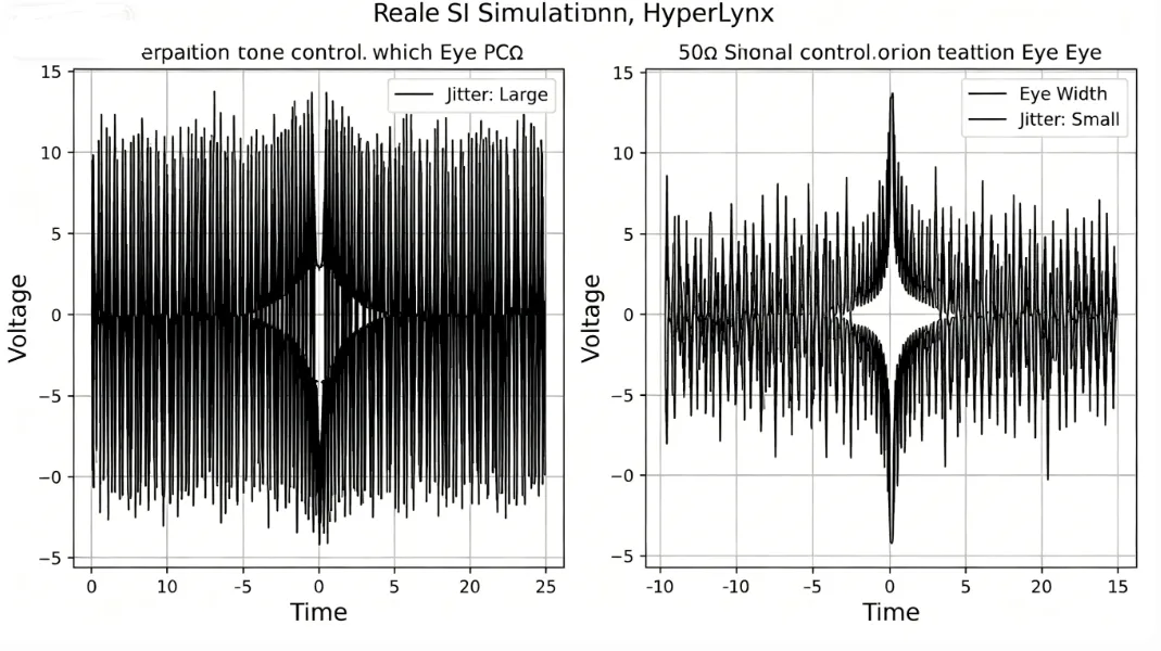
Troubleshooting starts with simulation: pre-layout S-parameters reveal reflections. Post-assembly, oscilloscopes capture eye patterns; closure indicates issues. Common fixes include trace serpentine for delay matching or ground vias for shielding. If integrity fails, analyze TDR for discontinuities. Iterative fab with coupons refines processes.
Conclusion
Impedance control unlocks signal integrity secrets in double-sided PCBs, transforming cost-effective boards into high-performance platforms. By grasping microstrip principles, precise calculations, and disciplined routing, engineers mitigate reflections and noise effectively. Standards like IPC-2141A, IPC-2221B, and IPC-6012E anchor these practices in proven methodologies. Prioritizing ground integrity and verification ensures double-sided PCB impedance matching success. As designs push frequencies, these strategies deliver reliability without complexity.
FAQs
Q1: What factors most influence impedance calculations double-sided PCB?
A1: Trace width, substrate thickness, dielectric constant, and copper thickness dominate microstrip impedance in double-sided PCBs. Engineers adjust width inversely to target Z0, while Er variations from material lots require coupons. Field solvers provide accuracy beyond approximations. Tight fab controls keep tolerances under 10%, vital for signal integrity double-sided PCB.
Q2: How does controlled impedance double-sided PCB improve high-speed performance?
A2: It minimizes reflections by matching source, trace, and load impedances, preserving waveform shape. In double-sided setups, solid ground pours reduce return path inductance, cutting EMI. This extends usable bandwidth, enabling reliable USB or LVDS signaling. Verification via TDR confirms compliance.
Q3: Why is signal integrity double-sided PCB harder than in multilayers?
A3: Lack of embedded planes heightens crosstalk and via effects in double-sided boards. Signals couple more to adjacent traces without shielding. Best practices like stitching and spacing compensate effectively for many designs.
Q4: What role do standards play in double-sided PCB impedance matching?
A4: Standards like IPC-2141A guide calculations and test methods for controlled impedance. They ensure consistency across design, fab, and qualification, reducing risks in high-speed double-sided PCB design.
References
IPC-2141A - Design Guide for High-Speed Controlled Impedance Circuit Boards. IPC, 2004
IPC-2221B - Generic Standard on Printed Board Design. IPC, 2003
IPC-6012E - Qualification and Performance Specification for Rigid Printed Boards. IPC, 2017


