ALLPCB


In the fast-paced world of electronics, designing printed circuit boards (PCBs) for high-frequency applications is a complex task. One key solution to ensure signal integrity and optimize performance is the use of sequential lamination vias. These specialized vias, often used in high-density interconnect (HDI) designs, play a crucial role in maintaining signal quality, especially in high-frequency environments. Additionally, they can reduce the number of layers needed in a PCB, which can lead to significant cost savings. In this blog, we’ll dive deep into what sequential lamination vias are, how they improve signal integrity for high-frequency applications, and why they are a smart choice for modern PCB designs.
What Are Sequential Lamination Vias?
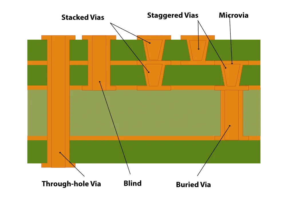
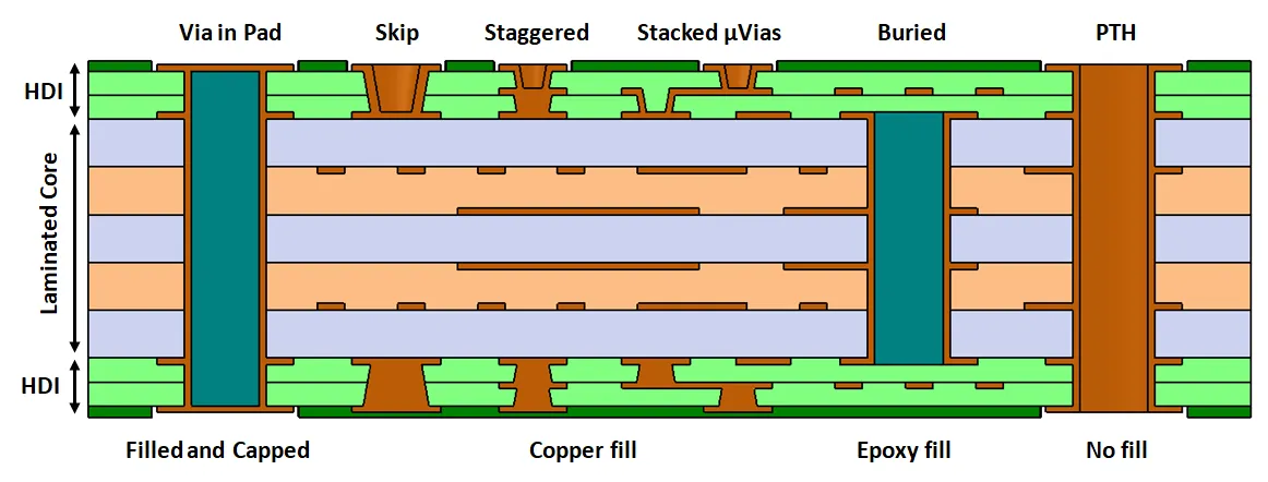
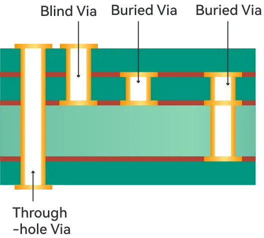
Sequential lamination vias are a type of via structure used in multilayer PCBs, particularly in HDI designs. Unlike traditional through-hole vias that span the entire thickness of the board, these vias are created through a step-by-step lamination process. This involves building the PCB in multiple stages, adding layers and vias incrementally. The result is a set of microvias, blind vias, or buried vias that connect specific layers without penetrating the entire board.
This manufacturing technique allows for finer traces and smaller via sizes, which are essential for high-frequency applications where space is limited, and signal integrity is paramount. By using laser drilling or other precision methods, sequential lamination creates highly reliable connections that minimize signal loss and interference.
Why Signal Integrity Matters in High-Frequency Applications
Signal integrity refers to the quality and reliability of an electrical signal as it travels through a PCB. In high-frequency applications—such as telecommunications, 5G networks, and advanced computing—signals operate at speeds often exceeding 1 GHz. At these frequencies, even small disruptions can lead to data loss, crosstalk, or electromagnetic interference (EMI).
Common challenges to signal integrity include:
- Impedance Mismatch: Variations in impedance can cause signal reflections, leading to data errors. For example, a mismatch of just 10 ohms in a 50-ohm system can degrade signal quality by over 20%.
- Signal Loss: High-frequency signals lose strength over longer traces due to dielectric losses and skin effect. Losses can reach up to 0.5 dB per inch at 10 GHz in standard materials.
- Crosstalk: Close proximity of traces can cause unwanted coupling, especially at high speeds, where interference levels can increase by 30% or more without proper shielding.
Sequential lamination vias address these issues by providing shorter, more direct signal paths and reducing the risk of interference, making them ideal for high-frequency designs.
How Sequential Lamination Vias Enhance Signal Integrity
Sequential lamination vias offer several advantages that directly contribute to better signal integrity in high-frequency applications. Let’s explore these benefits in detail.
1. Shorter Signal Paths
In traditional PCB designs, through-hole vias create long signal paths that can introduce delays and increase the risk of signal degradation. Sequential lamination vias, particularly microvias, connect only the necessary layers, reducing the via length. For instance, a microvia might span just 0.1 mm compared to a through-hole via of 1.6 mm in a standard board. This shorter path minimizes signal loss and latency, critical for signals operating at 5 GHz or higher.
2. Reduced Parasitic Effects
Vias can act as small capacitors or inductors, introducing parasitic effects that distort high-frequency signals. Sequential lamination vias, with their smaller size and precise placement, have lower parasitic capacitance and inductance. Studies show that microvias can reduce capacitance by up to 50% compared to through-hole vias, ensuring cleaner signal transmission.
3. Improved Impedance Control
Maintaining consistent impedance is vital for high-frequency signals. Sequential lamination allows for tighter control over via geometry and placement, reducing impedance variations. For a 50-ohm transmission line, using microvias can keep impedance deviations below 5%, compared to 10-15% with larger vias, significantly lowering signal reflections.
4. Minimized Crosstalk and EMI
By using blind and buried vias created through sequential lamination, designers can isolate high-frequency signals from other layers, reducing crosstalk. Additionally, the smaller via size and shorter stubs decrease EMI radiation. This is especially important in densely packed HDI boards where signal traces are often spaced less than 0.1 mm apart.
Sequential Lamination Vias and Cost Savings
Beyond their technical advantages, sequential lamination vias can also lead to cost savings in PCB design and manufacturing. While the initial setup for sequential lamination may seem complex, the long-term benefits often outweigh the costs.
1. Reducing the Number of Layers
High-frequency designs often require multiple layers to route signals and maintain isolation. Sequential lamination vias, with their ability to connect specific layers directly, allow designers to pack more functionality into fewer layers. For example, a design that might require 12 layers with traditional vias could be reduced to 8 layers using HDI techniques, cutting material and fabrication costs by up to 30%.
2. Optimizing Board Size
Smaller vias and finer traces enabled by sequential lamination mean that the overall board size can be reduced. A smaller PCB not only saves on material costs but also fits into compact devices, meeting the demand for miniaturization in industries like consumer electronics and medical devices.
3. Enhancing Reliability
Sequential lamination vias, especially microvias, are less prone to mechanical stress and thermal expansion issues compared to larger through-hole vias. This improved reliability reduces the need for costly rework or repairs, saving money over the product lifecycle. Data suggests that HDI boards with microvias have a failure rate of less than 0.5%, compared to 1-2% for traditional multilayer boards.
Applications of Sequential Lamination Vias in High-Frequency Designs
Sequential lamination vias are widely used in industries where high-frequency performance is non-negotiable. Here are some key applications:
- Telecommunications: In 5G infrastructure, where signals operate at frequencies up to 28 GHz, sequential lamination vias ensure minimal loss and high data rates.
- Automotive Electronics: Advanced driver-assistance systems (ADAS) rely on high-speed radar and sensors, requiring robust signal integrity provided by HDI designs.
- Consumer Electronics: Smartphones and wearables use compact HDI boards with sequential lamination to pack high-performance components into tiny spaces.
- Medical Devices: High-frequency imaging equipment benefits from the precision and reliability of microvias for accurate signal transmission.
Design Considerations for Sequential Lamination Vias
While sequential lamination vias offer numerous benefits, they require careful planning during the design phase to maximize performance and cost efficiency. Here are some practical tips for engineers:
1. Choose the Right Materials
High-frequency applications demand low-loss dielectric materials with a dielectric constant (Dk) below 3.5 and a dissipation factor (Df) under 0.005. These materials minimize signal loss and work well with the fine structures of sequential lamination vias.
2. Optimize Via Placement
Place vias strategically to avoid long stubs, which can act as antennas and cause signal reflections. For instance, aligning microvias directly under BGA (ball grid array) pads can reduce stub length by 80%, improving signal quality.
3. Balance Cost and Performance
While sequential lamination can reduce layer count, overusing microvias in non-critical areas can increase manufacturing complexity. Focus on using them for high-frequency signal paths while opting for simpler vias elsewhere.
4. Simulate Signal Integrity
Before finalizing the design, use simulation tools to model signal behavior at target frequencies. Tools can predict impedance mismatches or crosstalk, allowing adjustments to via size and spacing. For a 10 GHz signal, simulations might show a need to adjust via diameter from 0.2 mm to 0.15 mm for optimal performance.
Challenges of Implementing Sequential Lamination Vias
Despite their advantages, sequential lamination vias come with certain challenges that designers must navigate:
- Manufacturing Complexity: The step-by-step lamination process requires precision equipment and skilled technicians, which can increase initial costs.
- Thermal Management: Smaller vias may struggle to dissipate heat in high-power applications, necessitating additional thermal vias or heat sinks.
- Design Constraints: Sequential lamination often limits the aspect ratio of vias (depth-to-diameter), requiring careful planning to avoid reliability issues.
By partnering with an experienced PCB manufacturer, engineers can overcome these hurdles and fully leverage the benefits of this technology.
Conclusion: The Future of High-Frequency PCB Design
Sequential lamination vias are a game-changer for high-frequency applications, offering unmatched signal integrity and the potential for cost savings through reduced layer counts. As industries continue to push the boundaries of speed and performance, adopting HDI techniques with sequential lamination becomes not just an option but a necessity. Whether you’re designing for 5G networks, automotive systems, or compact consumer devices, these vias provide the precision and reliability needed to stay ahead in a competitive market.
By understanding their benefits, applications, and design considerations, engineers can create PCBs that meet the stringent demands of modern electronics. With the right approach, sequential lamination vias can help you achieve both technical excellence and cost efficiency in your next project.