 ALLPCB


Introduction
Automation PCBs power diverse components like microcontrollers, sensors, and motor drivers in industrial environments. These boards face dynamic loads that demand precise voltage stability to avoid system glitches or failures. Power integrity ensures the power distribution network delivers clean, consistent power across the entire board. Engineers must prioritize PDN design to handle transient currents and minimize noise in high-reliability applications. This article details the principles, strategies, and best practices for creating stable PDNs tailored to automation PCBs. By focusing on key elements like decoupling capacitors and power plane design, designers can enhance overall system performance.
What Is a Power Distribution Network and Why It Matters for Automation PCBs
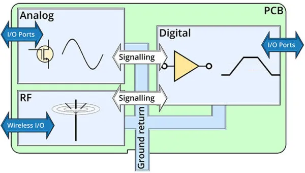
A power distribution network encompasses all conductive paths from the voltage regulator module to the power pins of integrated circuits, including traces, planes, vias, and capacitors. In PDN design, the goal is to maintain low impedance across a wide frequency range to supply current without excessive voltage droop. Automation PCBs operate in harsh conditions with frequent load changes from actuators and communication interfaces, making power integrity critical. Unstable power leads to issues like logic errors, electromagnetic interference, and reduced lifespan of components. Effective voltage regulation within the PDN prevents these problems and supports high-speed signal integrity. For electric engineers, understanding PDN behavior directly impacts the reliability of control systems in factories and robotics.
Power distribution network analysis reveals potential weaknesses early in the design cycle. Transient events, such as processor wake-ups, can draw amps in microseconds, causing voltage droop if the PDN lacks sufficient capacitance. In automation, where downtime costs are high, robust PDN design minimizes these risks. Standards like IPC-2221 provide foundational guidelines for material selection and layout that influence power delivery efficiency. Neglecting power integrity can cascade into signal integrity failures, amplifying noise across the board.
Core Technical Principles of Power Integrity in PDN Design
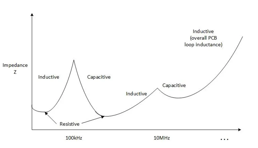
Power integrity hinges on controlling the PDN's impedance profile to stay below the target impedance curve. Target impedance is calculated as the maximum allowable DC voltage ripple divided by the peak transient current, ensuring voltage stays within tolerances. At low frequencies, bulk capacitors and planes dominate, while high frequencies rely on decoupling capacitors close to loads. Power plane design offers low inductance paths compared to trace networks, distributing current evenly and reducing resistance. Voltage droop occurs primarily from inductive voltage drops during current ramps, modeled as L di/dt. Engineers analyze the PDN using S-parameters to identify resonances where impedance peaks.
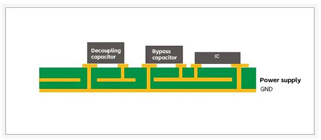
Decoupling capacitors act as local reservoirs, filtering high-frequency noise and supplying instant current during transients. Their effectiveness depends on equivalent series inductance and resistance, which vary with package size and mounting. In multi-layer boards, pairing power and ground planes closely minimizes loop inductance, a key factor in power plane design. Voltage regulation modules must be placed near high-current loads to shorten distribution paths. Power distribution network analysis tools simulate these interactions, predicting droop and noise before fabrication. Adhering to principles from IPC-2221 ensures designs meet thermal and electrical requirements for stable operation.
Minimizing voltage droop requires balancing DC resistance with AC impedance. Wide traces or planes handle steady-state currents without excessive IR drop, while strategic vias connect layers efficiently. Parasitic effects like via inductance become prominent at gigahertz frequencies, necessitating dense decoupling strategies. The PDN's overall health reflects in eye diagrams and jitter measurements during validation.
Best Practices for Stable PDN Design in Automation PCBs
Start PDN design with a clear current budget, allocating capacity per rail based on component datasheets. Use dedicated power planes for major voltage domains to achieve uniform distribution and low inductance. In power plane design, avoid splits under high-speed components to prevent impedance discontinuities. For voltage regulation, position point-of-load regulators adjacent to processors, minimizing trace lengths that amplify droop. Implement hierarchical decoupling: bulk capacitors near regulators, mid-range for board-level stability, and ceramic decaps within millimeters of IC pins. Select decoupling capacitors with low ESL, such as 0201 or 01005 sizes for high frequencies.
Power distribution network analysis should occur at schematic, pre-layout, and post-layout stages. Simulate worst-case transients to verify voltage droop stays below 5% of nominal. In automation PCBs, where mixed-signal environments prevail, segregate analog and digital power planes with proper stitching vias. IPC-2152 guidelines help size conductors for current carrying without overheating, critical for sustained loads from motors. Multiple ground returns and interplane capacitance further stabilize the PDN.
To minimize voltage droop, employ via farms for vertical current paths and fill unused spaces with power pours connected via stitching. Voltage regulation improves with synchronous buck converters for efficiency under varying loads. During layout, maintain consistent plane clearances and use odd-numbered layer counts for adjacent power-ground pairs. Post-design verification includes time-domain reflectometry for impedance checks. These practices ensure automation PCBs deliver reliable power under real-world stresses.
Troubleshooting Common Power Integrity Issues
Engineers often encounter excessive voltage droop during load steps, traced to insufficient decoupling or long regulator-to-load paths. Measure droop with high-bandwidth scopes at IC pins, comparing against simulations. Resonance peaks in PDN analysis indicate capacitor value mismatches; adjust arrays to fill impedance valleys. Power plane voids from routing can create high-impedance islands, resolved by adding redundant pours. Ground bounce couples noise into signals, mitigated by tighter plane spacing and enhanced stitching.
In automation prototypes, thermal hotspots from overloaded traces reveal current issues, addressed per IPC-2152 current charts. Simulate with accurate IBIS models for realistic transients. Iterative PDN design refines capacitor placement, often requiring board respins for validation.
Conclusion
Designing stable power delivery networks demands a holistic approach to PDN design, integrating power plane design, decoupling capacitors, and voltage regulation. By targeting low impedance and minimizing voltage droop through analysis, engineers achieve robust automation PCBs. Best practices like hierarchical decoupling and standard-compliant sizing prevent common pitfalls. Power distribution network analysis bridges simulation and reality, ensuring first-pass success. Automation systems benefit from these strategies, delivering uptime-critical performance. Prioritize power integrity early to unlock reliable, high-speed operation.
FAQs
Q1: What role do decoupling capacitors play in PDN design?
A1: Decoupling capacitors provide local charge storage to handle transient currents, keeping voltage stable during IC switching. Place them close to power pins with values spanning frequency ranges for broad coverage. In power plane design, they complement interplane capacitance to smooth ripples. Proper selection minimizes voltage droop in automation PCBs.
Q2: How does power plane design impact voltage regulation?
A2: Power planes offer low-impedance paths, reducing resistance and inductance for effective voltage regulation. Adjacent power-ground pairs enhance capacitance, stabilizing rails under load. Avoid splits to prevent current crowding. This approach is vital for PDN design in high-current automation applications.
Q3: Why is power distribution network analysis essential?
A3: PDN analysis predicts impedance profiles and voltage droop before fabrication, identifying decoupling needs. It verifies target impedance across frequencies, preventing noise coupling. Engineers use it to optimize layouts for automation PCBs, ensuring compliance with design margins.
Q4: What strategies minimize voltage droop in automation PCBs?
A4: Use wide planes, dense vias, and multi-tiered decoupling capacitors near loads. Position voltage regulators close to consumers and simulate transients. Stitch planes thoroughly to lower inductance. These tactics maintain stable power delivery during dynamic operations.
References
IPC-2221B — Generic Standard on Printed Board Design. IPC, 2003
IPC-2152A — Standard for Determining Current Carrying Capacity in Printed Board Design. IPC, 2009


