 ALLPCB


Introduction
In analog circuit design, PCB trace routing plays a critical role in maintaining signal integrity. Analog signals, unlike digital ones, operate with continuous voltage levels that are highly susceptible to degradation from environmental and internal noise sources. Proper PCB trace routing for analog circuits helps minimize PCB trace noise and PCB trace interference, ensuring reliable performance in applications like sensors, amplifiers, and data acquisition systems. Engineers must consider factors such as trace geometry, layering, and proximity to other signals during the layout phase. This article explores structured approaches to achieve low-noise routing, drawing on established engineering principles. By optimizing these elements, designers can enhance overall circuit accuracy and stability.
Why PCB Trace Routing Matters for Analog Circuits
Analog circuits demand precision, where even microvolt-level disturbances can compromise functionality. PCB trace noise arises from electromagnetic coupling, ground potential shifts, and external interference, directly impacting signal-to-noise ratios. In high-fidelity systems, such as audio processing or instrumentation, PCB trace interference can lead to distortion or measurement errors. Effective PCB trace routing analog paths separates sensitive signals from noise sources, preserving dynamic range. Industry standards like IPC-2221B emphasize conductor spacing and layout to support electrical performance. Ultimately, thoughtful routing translates to robust prototypes and production boards that meet performance specifications.
Understanding Noise and Interference Mechanisms
Noise in PCB traces manifests through several mechanisms, primarily crosstalk and electromagnetic interference. Crosstalk occurs when an aggressor trace induces unwanted voltage on a victim trace via capacitive or inductive coupling, proportional to their proximity and length. For analog signals, this coupling distorts waveforms, especially at higher frequencies where mutual inductance dominates. Ground noise, or ground bounce, propagates through shared return paths, coupling into analog lines if not isolated. External EMI from nearby power lines or clocks exacerbates PCB trace noise. Identifying these causes allows engineers to apply targeted mitigation during routing.
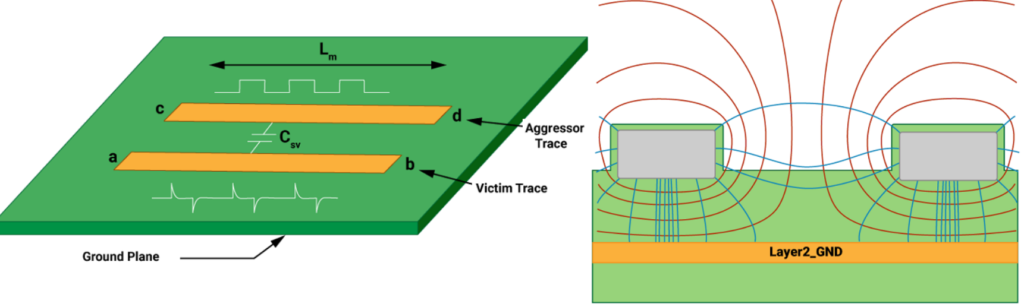
Inductive coupling strengthens with parallel trace runs over extended distances, creating loop antennas that pick up radiated fields. Capacitive coupling, conversely, depends on overlapping electric fields between traces on adjacent layers. In multilayer boards, via transitions can introduce impedance discontinuities, amplifying reflections and noise. PCB trace interference also stems from power distribution networks, where switching currents generate magnetic fields that link to nearby analog traces. Quantifying these effects requires simulation tools alongside empirical testing. Awareness of these physics guides routing decisions for cleaner signals.
Key Principles of Low-Noise PCB Trace Routing
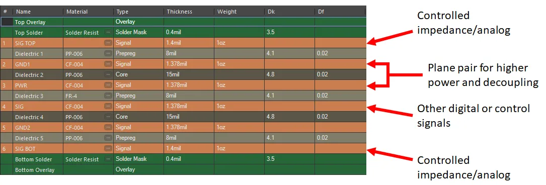
Start with layer stackup planning, dedicating inner layers for analog ground planes to shield signals. A solid ground plane under analog traces provides a low-impedance return path, reducing loop areas that act as noise antennas. Route analog signals on dedicated layers, avoiding splits or crossings with digital traces. Maintain consistent trace widths to control characteristic impedance, minimizing reflections that could fold back as noise. IPC-2221B outlines electrical clearance requirements to limit coupling between conductors. These foundational principles form the basis for interference-resistant layouts.
Trace length should be minimized to reduce exposure to coupling fields; shorter paths inherently lower accumulated noise. Avoid right-angle bends, opting for smooth 45-degree turns to prevent signal reflections and EMI radiation. Symmetry in routing preserves balance in differential analog pairs, canceling common-mode interference. Vias introduce parasitic inductance, so limit their use in critical analog paths or stitch grounds around them. Power traces must bypass analog sections entirely, preventing magnetic field intrusion. Adhering to these principles ensures PCB trace routing analog signals remains resilient.
Best Practices for Minimizing PCB Trace Noise and Interference
Partition the board into analog and digital zones during component placement, routing traces within their respective areas. Use guard traces—wide ground lines flanked by analog signals—to absorb stray fields and shunt noise to ground. Connect guard traces frequently to the analog ground plane via stitched vias. For single-ended signals, route adjacent to a ground trace forming a microstrip configuration, enhancing shielding. Increase spacing between traces carrying high dv/dt signals and sensitive analog lines, following voltage-based guidelines from IPC standards. These practices systematically suppress PCB trace interference.
In mixed-signal designs, employ split ground planes with a narrow bridge under the ADC interface to manage return currents without creating slots that radiate. Differential routing for balanced analog lines rejects common-mode noise effectively, provided pair symmetry is maintained. Filter high-frequency noise at trace entry points using capacitors tied to ground. Simulate routing post-layout to verify crosstalk levels remain below acceptable thresholds. During review, check for unbroken ground pours under analog sections. Implementing these steps yields layouts optimized for low PCB trace noise.
Employ via fencing around sensitive analog areas, where multiple ground vias form a Faraday cage-like barrier. Route clock and power traces orthogonally to analog lines on adjacent layers to minimize broadside coupling. For high-impedance analog inputs, widen clearances to prevent leakage currents. Thermal vias under power components dissipate heat without compromising analog isolation. Post-routing, perform design rule checks focused on spacing and plane integrity. These refined techniques elevate PCB trace routing for analog circuits to production-ready quality.
Troubleshooting Common Routing Issues in Analog PCBs
Unexpected noise spikes often trace back to shared ground returns between analog and digital sections. Solution: Implement separate analog and digital grounds, connecting at a single low-impedance point near the power supply. Crosstalk peaking at specific frequencies indicates parallel routing; reroute aggressors perpendicularly or add shielding. If simulations show excessive insertion loss, examine via count and lengths, optimizing with blind or buried vias where feasible. Measure PCB trace noise empirically using spectrum analyzers on prototypes, correlating to layout features. Iterative DRC and simulation resolve most issues before fabrication.
Ground loops manifest as 50/60 Hz hum; break them by star-point grounding or isolating supplies. In dense boards, trace crowding amplifies interference—prioritize analog routing first, then fill others. Review layer transitions for impedance steps causing ringing. These troubleshooting steps, grounded in systematic analysis, restore signal purity.
Conclusion
Mastering PCB trace routing for analog circuits demands a holistic approach to noise mitigation. By partitioning zones, leveraging ground planes, and applying guard techniques, engineers curb PCB trace noise and interference effectively. Standards like IPC-2221B provide essential guardrails for clearance and performance. Practical implementation through simulation and review ensures reliable outcomes. Analog designs thus achieve the fidelity required for demanding applications. Prioritizing these strategies in every layout elevates design quality.
FAQs
Q1: How does proper PCB trace routing for analog circuits reduce noise?
A1: PCB trace routing analog signals minimizes noise by separating sensitive paths from digital and power lines, using ground planes for shielding, and maintaining adequate spacing to limit coupling. Guard traces and short paths further suppress crosstalk and EMI. This structured approach preserves signal integrity per industry design guidelines, avoiding distortion in precision applications.
Q2: What causes PCB trace interference in analog designs?
A2: PCB trace interference stems from capacitive/inductive coupling between adjacent traces, ground bounce via shared returns, and radiated EMI from clocks or switches. Parallel routing amplifies these effects, while vias introduce discontinuities. Isolating analog sections and orthogonal layering counters these mechanisms effectively.
Q3: What are best practices for minimizing PCB trace noise during layout?
A3: Dedicate layers for analog grounds, route short symmetric paths, and employ guard traces tied to planes. Avoid right angles and minimize vias in signal paths. Partition board zones and verify with simulations to keep noise below thresholds. These steps align with electrical performance standards.
Q4: How can split ground planes help with PCB trace interference?
A4: Split ground planes isolate analog return currents from digital noise, connected at one point to prevent loops. This reduces coupling into analog traces while maintaining low impedance. Stitching vias around splits enhances shielding, a common tactic in mixed-signal boards.
References
IPC-2221B — Generic Standard on Printed Board Design. IPC, 2009
IPC-6012E — Qualification and Performance Specification for Rigid Printed Boards. IPC, 2017
J-STD-001GS — Requirements for Soldered Electrical and Electronic Assemblies. IPC, 2011


