 ALLPCB


Introduction
The electronics industry faces increasing pressure to adopt sustainable PCB manufacturing practices amid growing environmental regulations and consumer demands for greener products. Traditional PCB plating processes often involve hazardous materials that generate significant waste and pollution during production. Lead-free PCB plating options, such as OSP plating and direct metallization, emerge as key alternatives that balance performance with ecological responsibility. These environmentally friendly PCB finishes reduce the reliance on toxic chemicals while ensuring reliable solderability and assembly compatibility. For electric engineers designing high-density boards, understanding these alternatives proves essential for optimizing both functionality and sustainability. This article delves into their mechanisms, benefits, and implementation strategies aligned with factory processes.
Understanding PCB Plating and the Drive for Alternatives
PCB plating serves to protect exposed copper traces and pads from oxidation while facilitating solder joint formation during assembly. Conventional methods like hot air solder leveling with tin-lead alloys provided excellent solderability but introduced lead, a heavy metal restricted under global environmental directives. The shift to lead-free PCB plating addresses these concerns by eliminating lead and minimizing other harmful substances in plating baths. Environmentally friendly PCB finishes prioritize reduced water usage, lower chemical waste, and compatibility with high-temperature lead-free soldering processes. Factory-driven insights reveal that these alternatives also streamline production by simplifying waste treatment and disposal. Engineers must evaluate them based on board design, assembly methods, and long-term reliability requirements.
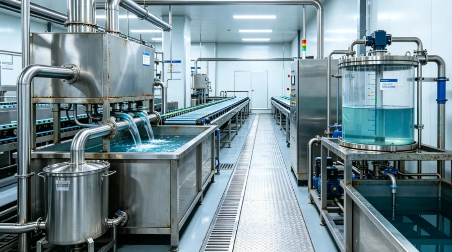
Traditional plating challenges include the generation of acidic effluents from electroless copper deposition, which requires extensive neutralization and disposal. Direct metallization bypasses this by applying a conductive seed layer directly onto drilled holes, avoiding palladium activators and copper etchant waste. OSP plating, meanwhile, coats copper with a thin organic layer that preserves solderability without metallic deposition. Both approaches align with sustainable PCB manufacturing goals by cutting resource consumption across the fabrication cycle. As production scales, these methods yield measurable reductions in operational footprints without compromising IPC class performance levels.
Technical Principles of Key Environmentally Friendly Options
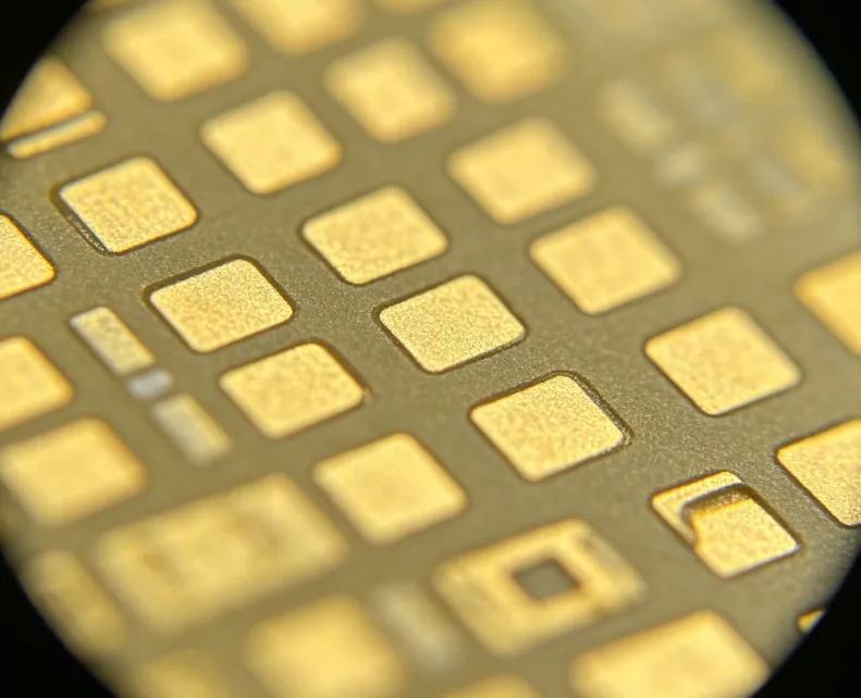
Lead-free PCB plating encompasses surface finishes applied post-patterning to ensure pad protection and wetting during reflow. OSP plating involves immersing cleaned copper surfaces in an organic solution, forming a molecular film typically 0.2 to 0.5 micrometers thick that prevents oxidation. This azole-based coating remains stable under ambient conditions and dissolves cleanly during soldering, exposing fresh copper for alloy formation. Its simplicity stems from no need for electrolytic or electroless metal layers, making it inherently low-waste. Factories appreciate OSP for its compatibility with multiple solder pastes and reflow profiles in lead-free assemblies.
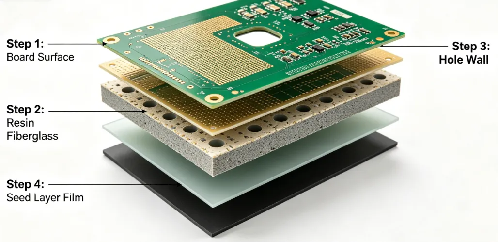
Direct metallization represents a paradigm shift in through-hole preparation and pattern plating. Instead of electroless copper, it deposits a catalytic polymer or carbon-graphite layer onto dielectric walls after desmear, enabling direct electrolytic copper buildup. This process eliminates formaldehyde and other toxic reducers used in traditional baths, substantially lowering effluent toxicity. The conductive layer ensures uniform plating coverage even in high-aspect-ratio vias, critical for modern multilayer boards. Environmental gains include reduced rinse water volumes and simplified chemical management, fostering sustainable PCB manufacturing at scale. Engineers note its efficacy in fine-line imaging where panel plating uniformity matters.
Other lead-free options like immersion tin complement these by displacing tin onto copper via redox reaction, offering a flat surface for fine-pitch components. However, OSP and direct metallization stand out for their minimal material use and process efficiency. Performance criteria for OSP align with IPC-4555, which specifies solderability and thickness uniformity for reliable factory outcomes. These principles ensure that environmentally friendly PCB finishes meet the demands of high-volume production without introducing reliability risks like black pad or whisker formation seen in some metallic alternatives.
Related Reading: OSP Finish on PCB: Pros and Cons
Practical Implementation and Best Practices
Selecting the right environmentally friendly PCB finish requires assessing board storage life, handling conditions, and assembly equipment. OSP plating suits cost-sensitive applications with short lead times, as its organic film degrades over extended exposure to humidity or contaminants. Factories mitigate this by implementing nitrogen-purged storage and rapid assembly protocols post-fabrication. Direct metallization excels in high-layer-count boards, where its waste reduction supports compliance with effluent discharge limits. Pairing it with optimized electroplating cycles minimizes overall process steps, enhancing throughput.
Best practices in sustainable PCB manufacturing emphasize process controls per J-STD-001 requirements for soldered assemblies. Engineers should specify finish thickness and test solder joint integrity via wetting balance or cross-section analysis early in design validation. For OSP, pre-dip cleaning with micro-etchants ensures uniform coating adhesion, preventing dewetting during reflow. Direct metallization benefits from precise desmear to avoid seed layer defects, which could propagate into plating voids. Integrating these into design rules reduces rework rates and supports IPC qualification levels for rigid boards.
Troubleshooting common issues reinforces factory reliability. OSP fingerprint contamination leads to inconsistent solderability, resolved by glove handling and vapor-phase cleaning. In direct metallization, over-polymerization causes poor throwpower, addressed by current density profiling during plating. These insights, drawn from production data, guide electric engineers toward robust specifications. Collaborative reviews between design and manufacturing teams optimize finish selection for specific thermal cycles and component densities.
Related Reading: A Quick Guide of OSP Surface Finished PCBs
Case Insights from Factory Perspectives
High-volume PCB fabricators report OSP adoption yielding streamlined workflows for consumer electronics, where multiple reflows demand repeatable solderability. One scenario involved transitioning from immersion silver to OSP, eliminating tarnish risks while cutting plating line maintenance by focusing on organic baths. Direct metallization proved transformative for automotive multilayer boards, enabling finer vias without electroless bath instability. These shifts not only advanced sustainable PCB manufacturing but also improved yield through fewer defect modes. Engineers leverage such factory-driven data to predict performance in lead-free environments.
Conclusion
Environmentally friendly PCB finishes like OSP plating and direct metallization redefine lead-free PCB plating by prioritizing ecological efficiency alongside engineering reliability. They address traditional process pitfalls, from hazardous waste to inconsistent coverage, fostering sustainable PCB manufacturing practices. Electric engineers benefit from their compatibility with modern assembly lines and standards-compliant outcomes. By integrating these options thoughtfully, production achieves reduced environmental impact without sacrificing quality. Future advancements will likely refine these processes further, solidifying their role in green electronics.
FAQs
Q1: What is OSP plating and its role in lead-free PCB plating?
A1: OSP plating applies a thin organic film to protect copper pads from oxidation in lead-free PCB plating processes. It ensures excellent solderability during reflow by dissolving upon heating, exposing pristine copper. This environmentally friendly PCB finish aligns with factory needs for low-cost, RoHS-compliant production. Its performance meets IPC-4555 criteria for uniformity and contact angle in wetting tests. Ideal for high-volume runs with short shelf life requirements.
Q2: How does direct metallization support sustainable PCB manufacturing?
A2: Direct metallization deposits a conductive layer directly on vias, bypassing toxic electroless copper steps central to sustainable PCB manufacturing. It reduces chemical waste and water usage, simplifying effluent treatment in factories. Compatible with fine-pitch designs, it maintains plating integrity per assembly standards like J-STD-001. Engineers favor it for high-aspect-ratio boards where traditional methods falter. Overall, it lowers operational costs while enhancing environmental compliance.
Q3: What factors determine the best environmentally friendly PCB finish for a project?
A3: Key factors include board complexity, storage duration, and reflow profile when choosing environmentally friendly PCB finishes. OSP suits flat surfaces and cost efficiency, while direct metallization excels in multilayer vias. Evaluate solder joint strength and handling protocols to avoid degradation. Factory alignment with IPC qualification specs ensures reliability. Consult process engineers early for optimal lead-free PCB plating selection.
Q4: Are lead-free PCB plating alternatives reliable for high-reliability applications?
A4: Yes, lead-free PCB plating alternatives like OSP and direct metallization deliver reliability in demanding sectors when properly qualified. They withstand multiple thermal cycles without compromising intermetallic formation. Standards such as J-STD-001 guide acceptance criteria for joints. Factories validate via accelerated aging and shear testing. These finishes support sustainable PCB manufacturing without reliability trade-offs.
References
- IPC-4555 — Performance Specification for Organic Solderability Preservatives. IPC, 2013
- J-STD-001H — Requirements for Soldered Electrical and Electronic Assemblies. IPC/JEDEC, 2020
- IPC-6012E — Qualification and Performance Specification for Rigid Printed Boards. IPC, 2017


