ALLPCB


Introduction
High-Density Interconnect (HDI) boards represent a cornerstone of modern electronics, enabling compact designs with superior performance in devices like smartphones, wearables, and medical equipment. These boards feature microvias, fine-line traces, and dense component placement, which demand exceptional manufacturing precision throughout the production cycle. HDI PCB depaneling, the process of separating individual boards from a production panel, introduces significant challenges due to the fragility of these features. Mechanical stresses or thermal effects can compromise board integrity, leading to yield losses and reliability issues downstream. This article delves into the core challenges of HDI PCB depaneling and outlines proven solutions, with a focus on achieving depaneling precision for fine pitch components. Factory insights reveal that selecting the right method is critical for maintaining quality in high-volume production.
What Is HDI PCB Depaneling and Why It Matters
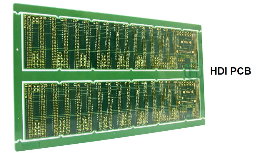
HDI PCB depaneling involves cleanly singulating multiple boards from a panel after fabrication and assembly, preserving the structural and electrical integrity of each unit. Traditional panels hold 6 to 24 boards, connected by tabs, V-scores, or routing, and improper separation can introduce microcracks or delamination. For HDI boards, this process matters profoundly because microvias and fine pitch components leave minimal margins for error, often with edge-to-component distances under 0.5 mm. In factory settings, depaneling defects account for up to 10 percent of rejects in dense designs, impacting throughput and cost. Compliance with standards like IPC-6012DS ensures that depaneled boards meet performance specifications for high-reliability applications. Ultimately, effective HDI PCB depaneling supports seamless transition to assembly and testing phases.
Key Challenges in HDI PCB Depaneling
HDI boards present unique hurdles in depaneling due to their thin substrates, typically 0.4 to 0.8 mm thick, and stacked microvias that are susceptible to stress-induced failures. Mechanical methods like routing or punching generate vibrations and forces that propagate through the panel, risking microvia damage from shear or tensile stress. Fine pitch components, such as BGAs with 0.3 mm or smaller pitches, sit perilously close to panel edges, amplifying the chance of chipping or lead deformation during separation. Warpage from prior lamination exacerbates alignment issues, leading to inconsistent cuts and burr formation. Dust and debris from mechanical processes further contaminate sensitive areas, necessitating extensive cleaning that can introduce additional handling risks. These factors underscore the need for depaneling precision in HDI manufacturing to avoid field failures.
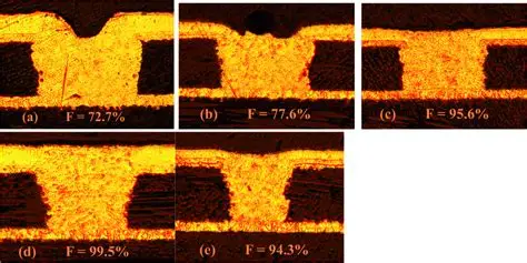
Microvia damage stands out as a primary concern, where even minor thermal or mechanical inputs can cause barrel cracks or resin separation at the via interface. Laser drilling creates these vias with diameters below 150 microns, but depaneling heat can induce charring or copper splash if not controlled. Fine pitch components demand edge finishes free of protrusions, as per IPC-A-600 acceptability criteria, to prevent solder joint defects during reflow. Panel fiducials often misalign due to thermal expansion mismatches in multi-layer HDI stacks, complicating automated routing paths. Factories report that unaddressed warpage leads to over 20 percent rework in extreme cases, highlighting the interplay of these challenges. Addressing them requires a shift from conventional approaches to specialized techniques.
Mechanical Depaneling Limitations for HDI Boards
Mechanical depaneling methods, including spindle routing, pizza cutters, and die punching, rely on physical contact that inherently introduces stress concentrations. Routing bits, spinning at high RPMs, create localized heating and vibration, which fracture brittle microvias in HDI structures. Punching suits simple panels but fails for complex outlines, often leaving tabs that require secondary trimming and increase handling damage. These processes generate fiberglass dust that embeds in solder masks, violating cleanliness standards and risking shorts under fine pitch components. Kerf widths exceed 1 mm, wasting panel real estate and limiting board count per panel. For HDI, where depaneling precision is paramount, mechanical methods yield inconsistent edges prone to burrs, demanding post-process deburring that adds cycle time.
Laser Depaneling for HDI: Technical Principles and Advantages
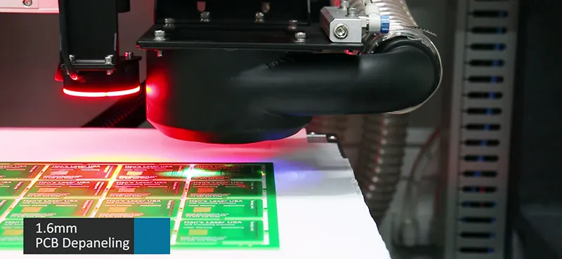
Laser depaneling for HDI employs focused beams, typically UV or green wavelengths, to ablate material in a non-contact manner, eliminating mechanical stress entirely. The process vaporizes copper, dielectric, and solder mask layer by layer, achieving kerf widths under 50 microns for maximal material efficiency. UV lasers minimize heat-affected zones (HAZ) to microns, preventing microvia damage by confining energy to the cut path. Precision optics and galvanometer scanners follow fiducial-aligned contours at speeds up to 200 mm/s, ideal for intricate HDI outlines. Fume extraction systems ensure dust-free operation, aligning with factory cleanliness protocols. This method excels in handling fine pitch components, maintaining standoffs as close as 100 microns without deformation.
The mechanism relies on photon absorption tailored to material properties: dielectrics like FR-4 ablate cleanly under short pulses, while copper reflects longer wavelengths inefficiently. Multi-pass strategies cut thicker stacks without residue buildup, crucial for HDI buildup layers. Vision systems correct for warpage in real-time, enhancing depaneling precision across varied panel conditions. Compared to mechanical routing, laser processes reduce cycle times for complex panels by avoiding tool changes. Factories integrating laser depaneling report yield improvements exceeding 15 percent for HDI runs. Thermal management, via pulse optimization, ensures compliance with IPC-A-600 edge quality requirements.
Best Practices for HDI PCB Depaneling
Select laser depaneling for HDI panels with microvia densities above Class 4, prioritizing UV sources for minimal HAZ on stacked vias. Optimize beam parameters, such as pulse duration below 20 ns and fluence matched to laminate Tg, to avoid resin charring near fine pitch areas. Incorporate fiducials at all corners and incorporate panel stiffeners to mitigate warpage during transport to depaneling stations. Perform inline metrology post-depaneling to verify edge straightness and absence of microcracks, aligning with IPC-6012DS qualification tests. Use hybrid tabs for mouse bites in mechanical fallback zones, but minimize their extent to reduce secondary laser passes. Train operators on assist gas flows to clear debris, ensuring consistent results across production shifts. These practices, drawn from factory optimization, boost throughput while safeguarding HDI integrity.
- Stress Introduction: Mechanical Depaneling - High (vibration, force); Laser Depaneling for HDI - None (non-contact)
- Precision: Mechanical Depaneling - ±100 microns; Laser Depaneling for HDI - ±20 microns
- Suitability for Fine Pitch: Mechanical Depaneling - Limited; Laser Depaneling for HDI - Excellent
- Dust Generation: Mechanical Depaneling - Significant; Laser Depaneling for HDI - Minimal (extracted fumes)
- Ideal for Microvias: Mechanical Depaneling - Poor; Laser Depaneling for HDI - Optimal
Troubleshooting Common HDI Depaneling Issues
In production, incomplete ablation manifests as recast layers on copper edges, detectable via cross-section analysis and mitigated by increasing overlap ratios. Component lift-off near fine pitches signals excessive panel flex; counter this with vacuum fixturing during laser runs. Microvia damage appears as via barrel separation under thermal cycling, traceable to HAZ penetration, resolved by wavelength selection for dielectric opacity. Warpage-induced misalignment triggers overcuts; employ adaptive optics software for dynamic correction. Post-depaneling inspections using dye penetrants reveal subsurface cracks early, preventing assembly escapes. Factories emphasize process DOE to baseline parameters, ensuring robustness across laminate variations.
Conclusion
HDI PCB depaneling demands a balance of precision and gentleness to protect microvias and fine pitch components from irreversible damage. While mechanical methods suffice for simpler boards, laser depaneling for HDI emerges as the superior solution, offering stress-free separation with unmatched accuracy. By adhering to standards like IPC-6012DS and implementing best practices such as optimized pulsing and fiducial alignment, manufacturers achieve higher yields and reliability. This approach not only addresses current challenges but scales with evolving HDI complexities in consumer and industrial electronics. Electrical engineers specifying these boards should prioritize depaneling capabilities in supplier qualifications to ensure end-product performance.
FAQs
Q1: What are the main challenges in HDI PCB depaneling?
A1: HDI PCB depaneling faces issues like microvia damage from stress, risks to fine pitch components near edges, and warpage affecting alignment. Mechanical methods exacerbate these with vibrations and burrs, while precision demands tight tolerances. Laser depaneling for HDI mitigates them through non-contact processing. Factories focus on these to maintain quality per IPC standards.
Q2: Why is laser depaneling preferred for HDI boards?
A2: Laser depaneling for HDI provides depaneling precision with narrow kerf widths and no mechanical stress, ideal for microvia protection. It handles complex outlines without dust, unlike routing that causes microcracks. UV lasers minimize thermal effects on fine pitch components. This results in cleaner edges and higher yields in production.
Q3: How does microvia damage occur during depaneling?
A3: Microvia damage in HDI PCB depaneling stems from mechanical shear or laser HAZ causing cracks or delamination. Fine pitch proximity amplifies risks from edge irregularities. Proper parameter tuning and non-contact methods prevent this. Inspections confirm integrity before assembly.
Q4: What best practices ensure depaneling precision for fine pitch components?
A4: Achieve depaneling precision by using fiducials, vacuum fixturing, and real-time vision correction in laser processes. Optimize for minimal HAZ to protect microvias. Post-cut metrology verifies edges. These steps align with factory standards for reliable HDI output.
References
[1] IPC-6012DS — Space and Military Avionics Applications Addendum to IPC-6012D, Qualification and Performance Specification for Rigid Printed Boards (ANSI store).