 ALLPCB


Introduction
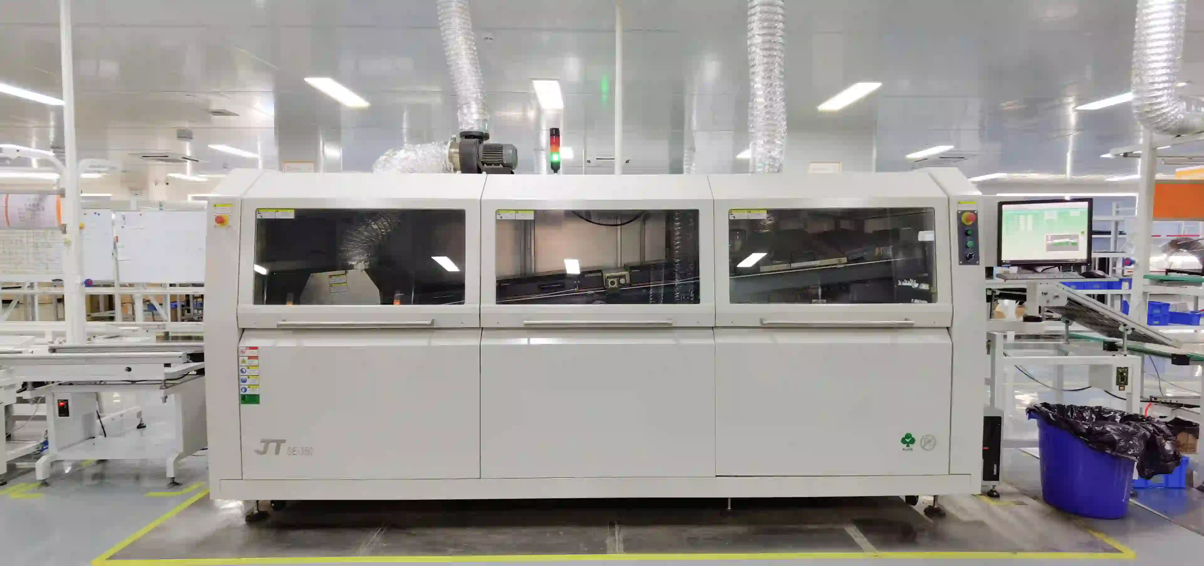
In PCB assembly, wave soldering remains a cornerstone process for through-hole technology, enabling high-volume production of reliable solder joints. Optimizing conveyor speed directly impacts process parameters like dwell time and immersion depth, balancing quality with throughput. Engineers often face challenges in achieving consistent hole fill and minimizing defects such as bridging or insufficient wetting. This article explores PCB wave soldering conveyor speed calculation, dwell time management, and strategies to enhance PCB wave soldering process efficiency. By fine-tuning these elements, manufacturers can boost PCB wave soldering throughput without compromising joint integrity. Practical adjustments grounded in engineering principles ensure repeatable results across production runs.
Understanding Conveyor Speed in Wave Soldering
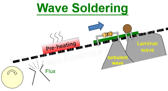
Conveyor speed dictates the duration a PCB spends in contact with the molten solder wave, fundamentally influencing solder joint formation. Too fast a speed reduces dwell time, leading to poor capillary action and incomplete hole fill, while excessive slowness risks overheating components and solder bridging. Industry practices target a dwell time of 2 to 4 seconds to allow sufficient heat transfer and wetting. This parameter interacts closely with wave geometry, including contact length and immersion depth. Engineers calculate speed based on desired contact duration using the formula: conveyor speed equals wave contact length divided by dwell time, with units converted appropriately for meters per minute. Proper synchronization with preheat zones prevents thermal shock, aligning the entire process for optimal performance.
Key Parameters Affecting Process Efficiency
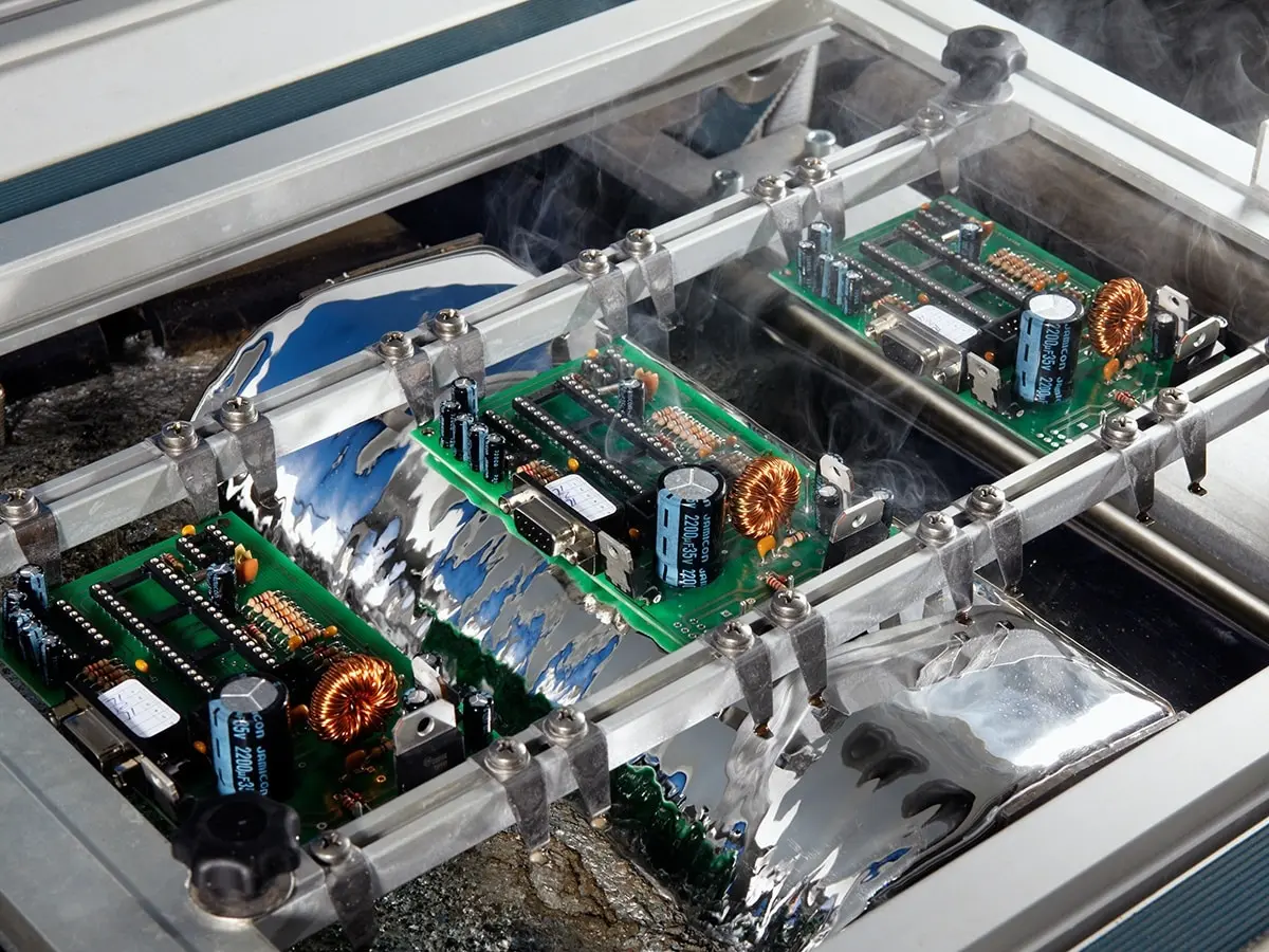
PCB wave soldering dwell time represents the critical window for solder to flow into vias and around leads via capillary forces. Immersion depth, typically set to about half the PCB thickness, ensures the solder wave contacts bottom-side pads without excessive splashing. Conveyor speed inversely scales dwell time, so a reduction from 1.5 to 1.0 meters per minute might extend contact by 50 percent for a fixed wave length. Throughput emerges as boards per hour, calculated roughly as conveyor speed multiplied by board width divided by effective board length including spacing. These variables demand profiling to verify compliance with standards like IPC-7530 for temperature and contact verification. Balancing them prevents common issues like icicles or non-wetting, directly elevating PCB wave soldering process efficiency.
PCB Wave Soldering Conveyor Speed Calculation
To perform PCB wave soldering conveyor speed calculation, first measure the solder wave contact length, often around 200 to 300 millimeters depending on machine nozzle design. Divide this by the target dwell time in seconds, then convert to meters per minute by multiplying by 60 and dividing by 1000. For instance, a 250 mm contact length and 3-second dwell yield a speed of approximately 1 meter per minute. Trial runs with oven-riders or high-speed cameras confirm actual contact, accounting for wave turbulence. Adjust for board thermal mass: thicker boards or dense copper require slower speeds to achieve internal temperatures for wetting. This methodical approach ensures predictable outcomes, minimizing variability across shifts.
Interplay of Dwell Time and Immersion Depth
PCB wave soldering dwell time must align with immersion depth to promote uniform solder penetration. Shallow immersion limits heat input, demanding longer dwell via slower conveyor speeds, whereas deeper contact accelerates filling but heightens bridging risk. Best practices recommend wave height not exceeding 50 percent of PCB thickness to maintain control. Flux activation during preheat enhances wetting, reducing required dwell for high-reliability joints per IPC-A-610 criteria. Engineers troubleshoot by monitoring hole fill percentage, targeting over 75 percent minimum. Iterative adjustments refine these parameters, sustaining high yields in mixed THT-SMT assemblies.
Enhancing Throughput Without Sacrificing Quality
PCB wave soldering throughput hinges on maximizing conveyor speed while upholding dwell time thresholds. Multi-board pallets increase effective density, allowing faster lines without individual board gaps. Dual-wave configurations, with a primary turbulent wave for wetting followed by a laminar cleanup wave, permit higher speeds by mitigating bridges. Preheat optimization reduces reliance on extended solder contact, freeing speed margins for output gains. Process efficiency improves through real-time monitoring of pot temperature and flux application uniformity. These tactics can elevate production rates by 20 to 30 percent in optimized setups, provided baseline profiling validates joint acceptability.
Best Practices for Optimization
Start with thermal profiling using multiple thermocouples to map topside and bottom-side temperatures, ensuring ramp rates stay below 4 degrees Celsius per second as guided by IPC-7530. Calibrate conveyor speed incrementally, verifying dwell with independent sensors rather than relying solely on machine readouts. Maintain consistent solder pot levels to stabilize immersion depth, and clean dross regularly to preserve wave shape. For lead-free alloys, target pot temperatures around 255 degrees Celsius paired with slower speeds for adequate hole fill. Document process windows for each board family, facilitating quick setups. These steps, rooted in J-STD-001 soldering requirements, yield robust processes resilient to material variations.
Troubleshooting Common Speed-Related Issues
Excessive bridging often signals overly slow conveyor speeds or deep immersion, prompting speed increases and wave height reductions. Insufficient wetting or poor hole fill indicates inadequate dwell, addressed by slowing the line and enhancing preheat. Speed inconsistencies arise from motor wear or misalignment, resolved through regular calibration and lubrication. Thermal profiling reveals hotspots from uneven dwell, guiding fixture adjustments for flat PCBs. Analyze rejects per IPC-A-610 to correlate defects with speed logs, enabling data-driven tweaks. Proactive maintenance prevents downtime, sustaining PCB wave soldering throughput.
Case Insights from Production Lines
In high-volume THT runs, reducing conveyor speed by 0.3 meters per minute for dense connector boards improved hole fill from 60 to 90 percent, though throughput dipped temporarily until pallet density rose. Mixed assemblies benefited from selective slower zones via fixtures, isolating critical areas. Profiling data showed dwell variations of up to 1 second across boards, corrected by uniform flux and speed locking. These adjustments aligned with standards, cutting defects by half. Engineers replicated successes by standardizing calculations across families. Such targeted optimizations exemplify practical efficiency gains.
Conclusion
Optimizing conveyor speed transforms PCB wave soldering from a bottleneck to a high-efficiency powerhouse. Precise PCB wave soldering conveyor speed calculation, coupled with dwell time and immersion depth control, unlocks superior throughput and joint reliability. Adhering to proven practices and standards ensures consistent results amid varying board designs. Engineers equipped with profiling tools and troubleshooting protocols achieve peak process efficiency. Implement these strategies to elevate production without quality trade-offs. Future advancements in sensor integration promise even finer control.
FAQs
Q1: How do you calculate PCB wave soldering conveyor speed for a target dwell time?
A1: Measure the solder wave contact length in millimeters, divide by the desired dwell time in seconds to get speed in mm/s, then convert to meters per minute. Typical dwell targets 2 to 4 seconds for most boards. Verify with profiling per IPC-7530 to account for actual dynamics. This ensures adequate wetting and hole fill, boosting PCB wave soldering process efficiency.
Q2: What is the ideal PCB wave soldering dwell time for lead-free soldering?
A2: Aim for 2 to 4 seconds, adjustable for board thickness and component density. Slower conveyor speeds extend dwell for high thermal mass boards, improving capillary fill. Monitor via sensors to avoid overheating. Balancing this enhances PCB wave soldering throughput while meeting J-STD-001 joint criteria.
Q3: How does immersion depth affect PCB wave soldering conveyor speed?
A3: Deeper immersion shortens required dwell time, allowing faster speeds and higher throughput. Limit to 50 percent of PCB thickness to prevent bridging. Pair with flux optimization for wetting. Fine-tuning both parameters per IPC-A-610 inspections maximizes process efficiency.
Q4: What factors influence PCB wave soldering throughput?
A4: Conveyor speed primarily drives output, moderated by dwell time needs and board spacing. Preheat uniformity and dual waves enable higher speeds without defects. Profile regularly to sustain gains. Optimized setups yield substantial efficiency improvements.
References
IPC-A-610 — Acceptability of Electronic Assemblies. IPC.
IPC-7530 — Guidelines for Temperature Profiling for Mass Soldering Processes. IPC.
J-STD-001 — Requirements for Soldered Electrical and Electronic Assemblies. IPC.
IPC-9502 — Printed Board Assembly Process Guideline for Electronic Components. IPC.


