ALLPCB


AllElectroHub Electronics News & Technical Insights
Say Goodbye to Sharp Edges - Inside ALLPCB’s Burr-Free PCB Process
Learn about PCB burrs, their causes, and impacts on electronics. Discover ALLPCB's multi-step process to ensure burr-free circuit boards for reliable performance.
Featured

Latest
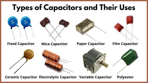
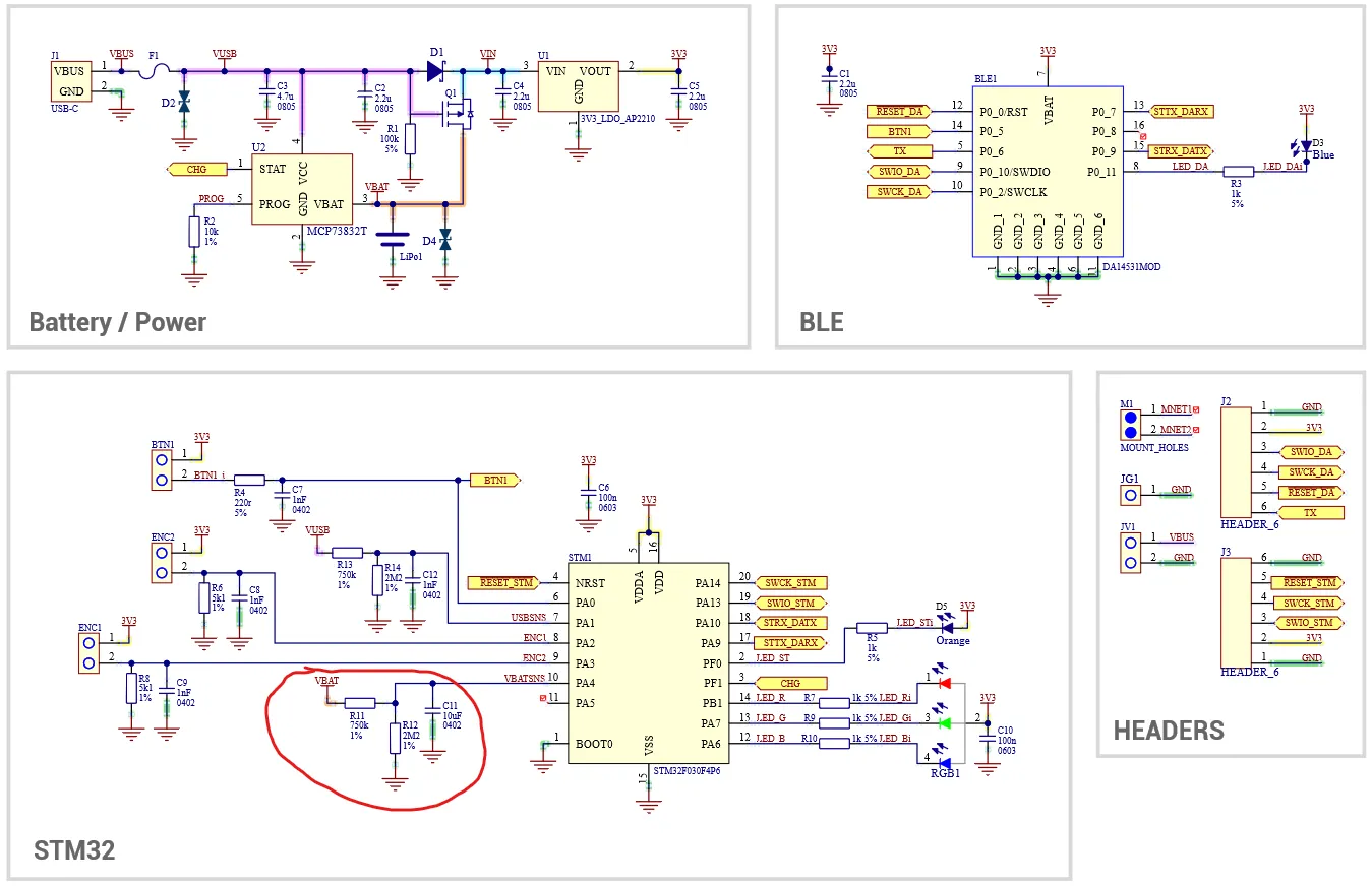
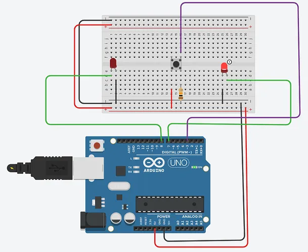
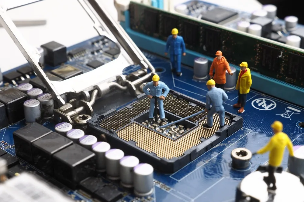
DIY Electronics: Essential Passive Components for Your First Project
Resistors and capacitors form the foundation for electronics hobbyist projects. This guide covers resistor color codes, common capacitor types, breadboard circuit tips and practical soldering techniques to help you complete your first builds successfully.
PCB Assembly
The Role of Flux in Lead Free HASL Soldering: Choosing the Right Formulation
Improve your production yields by selecting the ideal solder flux types for lead free HASL. This guide shows how no clean flux and activity levels impact wetting and overall PCB reliability.
PCB Knowledge
High Layer Count PCBs for High Speed Digital Applications: Design Considerations
High layer count PCBs help meet the routing density and reference plane needs of high speed digital PCB design. This guide explains signal integrity principles, impedance control PCB techniques, stackup planning, and key manufacturing considerations for consistent performance in multilayer boards.
PCB Knowledge
Simulating Stackup Performance for Signal Integrity Before Fabrication
Explore PCB stackup simulation to achieve optimal signal integrity. Simulate impedance and crosstalk to validate stackup performance prior to fabrication.
PCB Knowledge
Understanding Aspect Ratio in High Layer Count PCB Drilling
PCB aspect ratio directly affects drilling and plating quality in high layer count PCBs. This guide explains the technical factors, common manufacturing issues, and proven practices that help engineers achieve reliable results in complex multilayer boards.
PCB Knowledge
Lead Free HASL Thickness: Achieving Optimal Solder Joint Performance
Proper lead free HASL thickness supports strong solder joints during PCB assembly. This guide explains key factors, X ray fluorescence measurement methods, and practical controls that help maintain consistent coating quality and joint reliability in production.
PCB Knowledge