 ALLPCB


Introduction
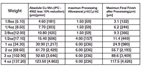
Designing printed circuit boards with heavier copper weights requires careful attention to layer arrangement and material selection. A 3 oz copper PCB stackup supports higher current carrying capacity compared with standard 1 oz constructions. Engineers often select this configuration for power electronics, motor drives, and industrial controls where thermal performance and voltage drop must remain within acceptable limits. The process begins with defining the number of layers, assigning signal and plane functions, and selecting dielectric materials that maintain consistent electrical and mechanical properties. Proper planning at this stage reduces the risk of manufacturing issues such as warpage or plating voids.
Why 3 oz Copper PCB Stackup Design Matters
Thicker copper layers improve current handling and heat dissipation, which becomes essential in applications drawing several amperes per trace. In a well planned PCB layer arrangement, power and ground planes made from 3 oz copper provide low impedance paths that stabilize voltage rails under load. Signal layers can remain thinner while still benefiting from the overall thermal mass of the board. This combination helps meet the demands of modern high power density designs without increasing board size. Industry standards such as IPC 6012E guide the qualification of such constructions to ensure reliability across temperature and environmental stresses. Designers who understand these trade offs can optimize both electrical performance and long term durability.
Technical Principles of PCB Layer Arrangement
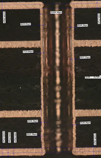
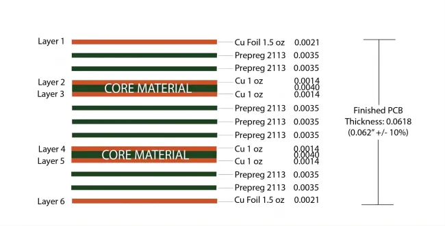
The stackup begins with a balanced distribution of copper to minimize mechanical stress during lamination and thermal cycling. Symmetric placement of 3 oz copper power and ground planes around the board center reduces the chance of warpage caused by coefficient of thermal expansion mismatch. Dielectric materials must be chosen for their glass transition temperature, dielectric constant, and loss tangent to support the required impedance targets on signal layers. Vias that connect through multiple 3 oz copper layers require larger drill diameters and controlled plating thickness to maintain structural integrity. Signal integrity considerations include managing return paths on adjacent planes and controlling trace width to achieve the desired characteristic impedance. Thermal vias and copper pours further distribute heat away from high dissipation components.
PCB Dielectric Materials and Their Role
Dielectric selection directly influences both electrical performance and manufacturability in 3 oz copper designs. Materials with higher thermal conductivity help conduct heat away from traces and planes while maintaining insulation between layers. The thickness of each dielectric layer must be controlled to achieve target impedance values on signal layers routed over or between 3 oz copper planes. Prepreg and core materials are selected to match the overall expansion characteristics of the copper, reducing internal stresses. In multilayer constructions, the number and placement of dielectric layers also affect the board's ability to withstand reflow temperatures without delamination. Consistent material properties across production lots support repeatable electrical results.
Practical Solutions and Best Practices
Begin the design process by calculating the required copper weight based on maximum current, allowable temperature rise, and trace length. Use simulation tools to model current density and thermal distribution before finalizing the PCB layer arrangement. Maintain symmetry in the stackup so that 3 oz copper power and ground planes mirror each other above and below the center. Specify dielectric thicknesses that allow standard impedance calculations while accommodating the increased height of 3 oz copper. Incorporate sufficient clearance around vias and consider filled or capped vias when high current paths must transition between layers. Review the design against IPC A 600K acceptability criteria to ensure manufacturability.
PCB Signal Layers, Power and Ground Planes Integration
Signal layers typically use 1 oz or 0.5 oz copper to preserve fine line resolution, while power and ground planes utilize 3 oz copper for low resistance. Careful assignment of reference planes adjacent to high speed signals maintains return path integrity and reduces electromagnetic interference. When routing signals over 3 oz planes, account for the increased dielectric spacing that may result from the thicker copper. Power distribution networks benefit from solid 3 oz planes that can carry large currents with minimal voltage drop. Ground planes also serve as heat spreaders, improving overall thermal performance when connected to chassis or heatsinks through appropriate mounting features.
Conclusion
Effective 3 oz copper PCB stackup design combines electrical, thermal, and mechanical considerations into a single coherent structure. Attention to layer arrangement, dielectric properties, and copper balance produces boards that meet both performance and reliability requirements. Following established industry practices helps designers avoid common pitfalls such as excessive warpage or plating defects. The result is a robust platform suitable for demanding power applications.
FAQs
Q1: What factors determine the choice of 3 oz copper PCB stackup design for high current applications?
A1: Engineers evaluate maximum current per trace, allowable temperature rise, board size constraints, and the need for low impedance power distribution when selecting a 3 oz copper construction. The arrangement of signal layers relative to power and ground planes also influences the final decision.
Q2: How does PCB dielectric material selection affect impedance control in a 3 oz copper stackup?
A2: Dielectric thickness and dielectric constant determine the characteristic impedance of traces routed on signal layers. Consistent material properties across the board help maintain target impedance values even when thicker 3 oz copper planes increase overall board height.
Q3: What considerations apply to PCB power and ground planes when using 3 oz copper?
A3: Power and ground planes benefit from the reduced resistance and improved thermal spreading of 3 oz copper. Designers must still ensure adequate clearance for vias and maintain symmetry to prevent mechanical distortion during manufacturing and operation.
Q4: How can PCB layer arrangement minimize warpage in 3 oz copper designs?
A4: Balanced copper distribution on both sides of the board center, combined with matched dielectric materials, reduces differential expansion. Following guidelines in IPC 6012E supports consistent results across production.


