ALLPCB


Introduction
Silkscreen, also known as the legend layer, plays a crucial role in printed circuit board manufacturing by providing essential markings for component identification, polarity indicators, and assembly references. Engineers often face the decision between manual and automated silkscreen methods, each offering distinct trade-offs in precision, cost, and throughput. This choice impacts overall PCB quality, especially in high-reliability applications where clear legibility is paramount. Automated silkscreen precision stands out for demanding production environments, while manual approaches suit smaller scales. Additionally, liquid photo imaging emerges as a viable alternative for specific scenarios. Understanding these methods helps electric engineers select the optimal process aligned with design requirements and production volumes.
What Is Silkscreen and Why It Matters in PCB Manufacturing
Silkscreen involves applying durable polymer ink to the PCB surface, typically over the solder mask, to create text, logos, and symbols that survive assembly and operational stresses. These markings facilitate troubleshooting, rework, and compliance verification during the PCB lifecycle. In factory settings, silkscreen quality directly influences assembly efficiency and defect rates, as unclear legends can lead to misplacement or errors. Industry standards like IPC-A-600 define acceptability criteria for markings, ensuring legibility under various classes from prototype to high-reliability boards. Poor silkscreen can compromise traceability, making it a critical step in the manufacturing flow. For electric engineers, reliable silkscreen supports signal integrity analysis and field maintenance.
The Manual Silkscreen Process
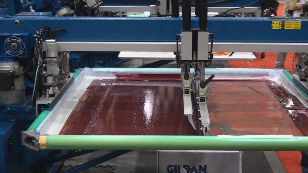
Manual silkscreen uses a hand-held squeegee to push ink through a mesh stencil aligned over the PCB panel. Operators visually position the board, apply uniform pressure, and cure the ink via oven or UV exposure. This method requires skilled labor to minimize misalignment and ink bleeding. Setup involves stretching emulsion-coated mesh, exposing it to artwork, and washing out the image to form the stencil. Factories often reserve manual processes for low-volume runs due to their flexibility in handling custom designs.
Manual silkscreen advantages include low initial setup costs and quick turnaround for prototypes or one-off boards, making it economical without heavy capital investment. It allows immediate adjustments for unique panel shapes or small batches where automation proves inefficient. However, manual silkscreen disadvantages encompass inconsistent line widths, potential for pinholes, and operator fatigue leading to variability across panels. Precision suffers from human error in alignment, often limiting minimum feature sizes to broader tolerances unsuitable for dense layouts. Throughput remains low, typically handling only hundreds of prints per shift compared to automated systems.
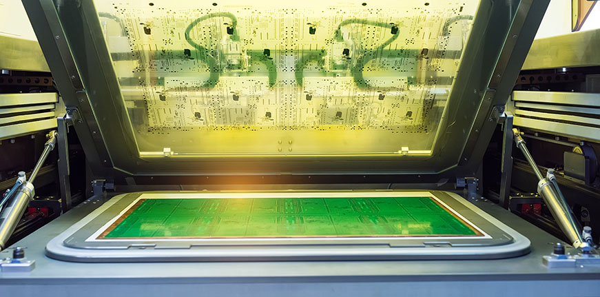
Automated Silkscreen Process and Its Precision Advantages
Automated silkscreen employs precision machinery with CCD cameras for optical registration, ensuring sub-micron alignment between stencil and board fiducials. The system clamps the panel, floods ink evenly, and squeegees with controlled speed and pressure before automated curing. Multi-station lines handle double-sided or multi-color printing, integrating inline inspection for defects like bridging or voids. This factory-driven approach scales seamlessly for medium to high volumes, reducing cycle times significantly.
Automated silkscreen precision excels in maintaining uniform ink deposition, achieving finer line resolutions down to 4 mils reliably across large panels. Vision systems detect and correct offsets in real-time, minimizing rejects and enhancing yield. Ink viscosity and squeegee angle are programmed for optimal flow, preventing common manual issues like smearing. For electric engineers designing compact boards, this consistency supports tighter component spacing without legend overlap. Overall, automation aligns with performance specifications in IPC-6012, where marking durability under thermal cycling is verified.
Liquid Photo Imaging: An Advanced Alternative
Liquid photo imaging applies a photosensitive epoxy ink via spin coating or spray, followed by UV exposure through a phototool and chemical development to reveal the image. This dry-film-like process cures the remaining ink, bonding it firmly to the board surface. Unlike screen printing, LPI avoids stencil wear, enabling repeated high-resolution imaging without remakes. Factories use it post-solder mask to leverage similar equipment lines.
Use liquid photo imaging when designs demand superior resolution for fine-pitch components or text smaller than traditional screen limits, such as in high-density interconnect boards. It provides sharper edges and better adhesion, resisting cracking during reflow or flexing. However, it requires cleanroom conditions to prevent contamination during coating and development. For prototypes, LPI adds steps but ensures compliance with stringent legibility per IPC-A-600. Electric engineers benefit from its precision in multilayer stacks where space constraints challenge conventional methods.
Comparing Manual, Automated, and LPI Silkscreen Methods
Precision: Manual - Moderate, operator-dependent; Automated - High, vision-aligned
Production Volume: Manual - Low (prototypes); Automated - Medium to high; LPI - Medium, high-density.
Cost: Manual - Low setup, high labor; Automated - High equipment, low per-unit; LPI - Moderate, process-intensive.
Minimum Line Width: Manual - 6-8 mils typical; Automated - 4 mils reliable; LPI - 3-4 mils achievable.
Standards Compliance: Manual - Meets basic IPC classes; Automated - IPC-6012 durability; LPI - Superior legibility IPC-A-600.
Manual silkscreen advantages disadvantages highlight its niche for cost-sensitive, low-quantity needs, but scalability limits push toward automation. Automated systems dominate for consistency, while LPI addresses resolution gaps.
Best Practices for Selecting the Right Silkscreen Method
Evaluate production volume first: opt for manual silkscreen advantages disadvantages favoring low runs under 100 panels to avoid overkill. For volumes exceeding 500, leverage automated silkscreen precision to cut costs and boost quality control. Assess design density; use liquid photo imaging when trace spacing or text drops below 4 mils, ensuring no encroachment on pads. Always verify ink compatibility with board finish and cure profiles to meet IPC-4781 qualification for adhesion and resistance. Conduct inline optical checks post-printing to catch defects early. Collaborate with manufacturing early to balance cost, lead time, and performance.
In high-reliability sectors, prioritize methods supporting Class 3 per IPC-A-600, where markings withstand environmental stresses without fading.
Factory Insights: Troubleshooting Common Silkscreen Issues
Factories encounter ink bleeding in humid conditions, often mitigated by pre-baking panels and controlling viscosity. Misalignment in manual processes stems from poor fiducial design; automate where possible. LPI development residues require thorough rinsing to prevent shorts. Yield data from production lines shows automated setups reducing defects by focusing on root causes like stencil tension. Engineers should specify tolerances upfront, aligning with J-STD standards for process control.
Conclusion
Choosing between manual and automated silkscreen hinges on balancing precision, volume, and cost, with each method serving distinct factory needs. Manual offers flexibility for prototypes despite its variability, while automated silkscreen precision drives efficiency in scale. Liquid photo imaging fills the gap for fine-feature demands, enhancing overall PCB reliability. Adhering to standards like IPC-A-600 ensures markings endure the full product lifecycle. Electric engineers gain from informed selection, optimizing assembly and maintenance.
FAQs
Q1: What are the manual silkscreen advantages disadvantages for PCB production?
A1: Manual silkscreen advantages include low setup costs and suitability for small prototypes, allowing quick changes without machinery. Disadvantages involve lower precision from human variability, slower throughput, and higher defect risks like misalignment or bleeding. It suits low-volume runs but struggles with consistency for production boards, often requiring rework. Factories recommend it only when volumes stay under a few hundred panels.
Q2: How does automated silkscreen precision benefit high-volume PCB manufacturing?
A2: Automated silkscreen precision uses CCD alignment for sub-mil accuracy, ensuring uniform ink and minimal defects across panels. It handles large runs efficiently, reducing labor and scrap rates while meeting IPC tolerances. Vision inspection catches issues inline, supporting Class 2/3 quality. This method excels for medium volumes, providing sharper legends than manual without added steps.
Q3: When to use liquid photo imaging for PCB silkscreen?
A3: Use liquid photo imaging when designs feature fine text or dense layouts under 4 mils, where screen printing falters. It delivers high-resolution images via photolithography, ideal for HDI boards needing sharp, durable markings. Post-solder mask application leverages clean surfaces for better adhesion. Avoid for very low volumes due to coating complexity, but it aligns with precision demands in advanced assemblies.
Q4: What standards govern silkscreen quality on PCBs?
A4: IPC-A-600 sets acceptability for legend legibility and defects, classifying from prototype to mission-critical. IPC-6012 specifies performance under thermal and mechanical stress. These ensure markings remain intact post-assembly, aiding traceability. Compliance verifies via visual and adhesion tests in factories.
References
- IPC-A-600K - Acceptability of Printed Boards. IPC, 2020
- IPC-6012E - Qualification and Performance Specification for Rigid Printed Boards. IPC, 2017
- IPC-4781 - Qualification and Performance of Permanent Solder Mask. IPC, 2019