 ALLPCB


Introduction
In the precision-driven world of PCB manufacturing and assembly, maintaining accurate temperature control is essential for ensuring reliability and performance. IR temperature sensors enable non-contact temperature measurement, allowing engineers to monitor thermal profiles without physically touching sensitive components or boards. This approach is particularly valuable during PCB testing phases, where traditional contact methods like thermocouples can introduce errors or damage delicate assemblies. Infrared thermography provides real-time thermal imaging, revealing hotspots, uneven heating, and potential defects that could compromise functionality. As electric engineers focus on optimizing processes aligned with industry standards, integrating IR temperature sensors streamlines quality control and reduces failure risks in high-volume production.
What Are IR Temperature Sensors and Why Do They Matter for PCB Testing?
IR temperature sensors detect infrared radiation emitted by objects, converting it into temperature readings based on the Stefan-Boltzmann law. These devices operate in the infrared spectrum, typically from 8 to 14 micrometers, where most terrestrial materials emit peak radiation at operational temperatures. In PCB testing, they excel in non-contact scenarios, such as monitoring reflow soldering zones or inspecting assembled boards for thermal anomalies. Contact sensors often alter the thermal equilibrium or fail in dynamic environments like conveyor systems, whereas IR sensors maintain process integrity. Their relevance grows with denser PCB designs, where components like BGAs and fine-pitch ICs demand precise thermal management to prevent issues like delamination or solder joint voids.
The factory-floor adoption of IR temperature sensors aligns with quality assurance goals, enabling proactive detection of variances before they escalate. Engineers benefit from their speed, capturing data across entire boards via thermal imaging arrays. This capability supports compliance with thermal performance specifications, reducing rework and enhancing yield rates.
Technical Principles Behind IR Temperature Sensors
Infrared thermography relies on the principle that all objects above absolute zero emit infrared radiation proportional to their temperature and surface emissivity. Sensors use a lens to focus this radiation onto a detector, often a microbolometer array, which generates a voltage signal processed into a temperature map. Emissivity, a material property between 0 and 1, critically affects accuracy; for instance, oxidized copper on PCBs has higher emissivity than bare metal, requiring adjustments for precise readings. Field of view and distance also influence spot size resolution, demanding careful sensor positioning to avoid averaging errors over non-uniform surfaces.
Environmental factors like ambient temperature, humidity, and reflective surfaces can introduce noise, necessitating shielded setups or dual-band sensors for compensation. Calibration against blackbody references ensures traceability, vital for repeatable PCB testing. In practice, these principles allow thermal imaging to visualize gradients, identifying stress points from CTE mismatches between layers.
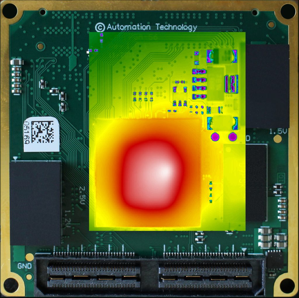
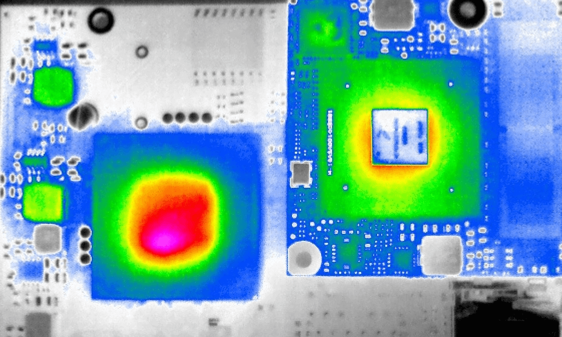
Applications of IR Temperature Sensors in PCB Testing
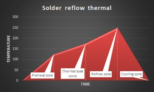
During reflow soldering, IR temperature sensors validate profile adherence by mapping conveyor temperatures and board-level heating without obstructing airflow. This non-contact temperature measurement captures peak temperatures and ramp rates, essential for preventing component damage in lead-free processes. Post-reflow, thermal imaging detects soldering defects like cold joints or bridging through localized overheating signatures.
In quality control, IR sensors inspect for warpage or delamination by observing thermal expansion responses under controlled heating, aligning with IPC-6012DS qualification requirements for rigid printed boards. They also evaluate component-level hotspots during functional testing, revealing power dissipation issues early. JEDEC JESD51-2A outlines thermal test methods where IR sensors supplement traditional transducers for junction-to-case characterizations.
For incoming inspection, scanning bare boards identifies laminate inconsistencies via uneven cooling patterns after bake-out. In high-reliability sectors, these tools support accelerated life testing by monitoring thermal cycling without invasive probes.
Best Practices for IR Temperature Sensors in PCB Testing
Select sensors with appropriate spectral response and resolution matching PCB materials, such as those handling emissivity from 0.9 for solder masks to 0.6 for metallized traces. Calibrate regularly using reference sources traceable to standards, and document emissivity tables for common substrates. Position sensors perpendicular to the surface at optimal distances to minimize parallax errors, often 30-50 cm for handheld units or fixed mounts in production lines.
Integrate with data logging software for trend analysis, correlating thermal data with electrical tests for comprehensive PCB testing. Employ averaging modes for noisy environments and active cooling to stabilize sensor housings during prolonged use. Factory protocols should include baseline scans of known good boards to establish delta-T thresholds for defect flagging.
Avoid direct sunlight or heat sources interfering with readings, and use protective enclosures in dusty assembly areas. Training operators on interpreting thermal images prevents false positives from reflections.
Troubleshooting Common Issues with IR-Based PCB Testing
Uneven temperature readings often stem from incorrect emissivity settings; verify against material datasheets and test strips. Hotspots appearing on copper planes may indicate voids under masks rather than true failures, requiring cross-verification with X-ray. Reflective surfaces causing low readings demand matte coatings or angle adjustments.
In reflow monitoring, conveyor speed variances skew profiles, so synchronize sensor triggers with encoders. If thermal imaging shows symmetric gradients but functional failures persist, check for intermittent issues needing powered testing. Adhering to J-STD-020E guidelines for reflow sensitivity helps contextualize thermal data against moisture-induced defects.
Persistent drift signals sensor fouling; routine lens cleaning restores performance. Document anomalies with overlaid visible-IR images for root cause teams.
Conclusion
IR temperature sensors revolutionize non-contact temperature measurement in PCB testing, offering precision and efficiency for modern assembly lines. From reflow validation to defect detection via infrared thermography, they empower electric engineers to uphold thermal integrity without compromising processes. Best practices in calibration and setup maximize accuracy, while troubleshooting ensures reliable insights. Integrating these tools enhances compliance with key standards, ultimately boosting PCB reliability and production yields.
FAQs
Q1: What advantages do IR temperature sensors offer over thermocouples in PCB testing?
A1: IR temperature sensors provide non-contact temperature measurement, avoiding physical attachment that could damage fine-pitch components or alter heat flow. They enable full-board thermal imaging for hotspot detection during reflow or functional tests. This speeds up PCB testing cycles and supports real-time adjustments in production. Factory engineers appreciate their scalability for inline quality control without probe wear issues.
Q2: How does emissivity impact accuracy in infrared thermography for PCBs?
A2: Emissivity measures how efficiently a surface emits infrared radiation compared to a blackbody. PCBs vary with solder mask (high emissivity) versus bare copper (low), requiring sensor adjustments for true readings. Incorrect settings lead to under- or overestimation by 20-50 degrees Celsius. Calibrate per material and validate with spot checks to align with thermal standards.
Q3: Can IR sensors detect soldering defects in assembled PCBs?
A3: Yes, infrared thermography reveals defects like cold joints or voids through abnormal temperature gradients during powered testing. Hotspots indicate bridging or poor connections, while cooler areas signal opens. Non-contact scanning post-reflow identifies issues missed by visual inspection. This method integrates into PCB testing workflows for high-reliability assurance.
Q4: What role do industry standards play in IR-based PCB thermal testing?
A4: Standards like IPC-6012DS define performance specs including thermal endurance, guiding IR sensor use for qualification. JEDEC JESD51-2A permits IR for thermal characterizations, ensuring consistent data. They promote standardized profiles and thresholds, aiding factory compliance and defect prevention in non-contact temperature measurement.
References
IPC-6012DS — Qualification and Performance Specification for Rigid Printed Boards. IPC, 2020
JEDEC JESD51-2A — Integrated Circuits Thermal Test Method Environmental Conditions - Natural Convection. JEDEC, 2008
IPC/JEDEC J-STD-020E — Moisture/Reflow Sensitivity Classification for Nonhermetic Solid State Surface Mount Devices. IPC/JEDEC, 2014


