 ALLPCB


Introduction
Automotive electronics form the backbone of modern vehicles, powering everything from engine control units to advanced driver-assistance systems. These components must withstand extreme conditions like high temperatures, vibrations, and moisture exposure, where failures can lead to safety risks or costly recalls. X-ray inspection automotive emerges as a critical non-destructive testing method to verify internal integrity without compromising the assembly. By revealing hidden defects in solder joints and components, it directly supports automotive electronics quality assurance. This article explores how x-ray inspection for vehicle components integrates into quality control processes, emphasizing its role in harsh environment testing.
Factory-driven protocols prioritize x-ray inspection for high-density assemblies common in vehicles. Electric engineers rely on this technique to correlate manufacturing defects with long-term field performance. As vehicles incorporate more electronics, the demand for robust inspection grows, making x-ray a standard in production lines. Understanding its application ensures compliance with reliability expectations in automotive PCB inspection.
What Is X-Ray Inspection and Why It Matters in Automotive Electronics
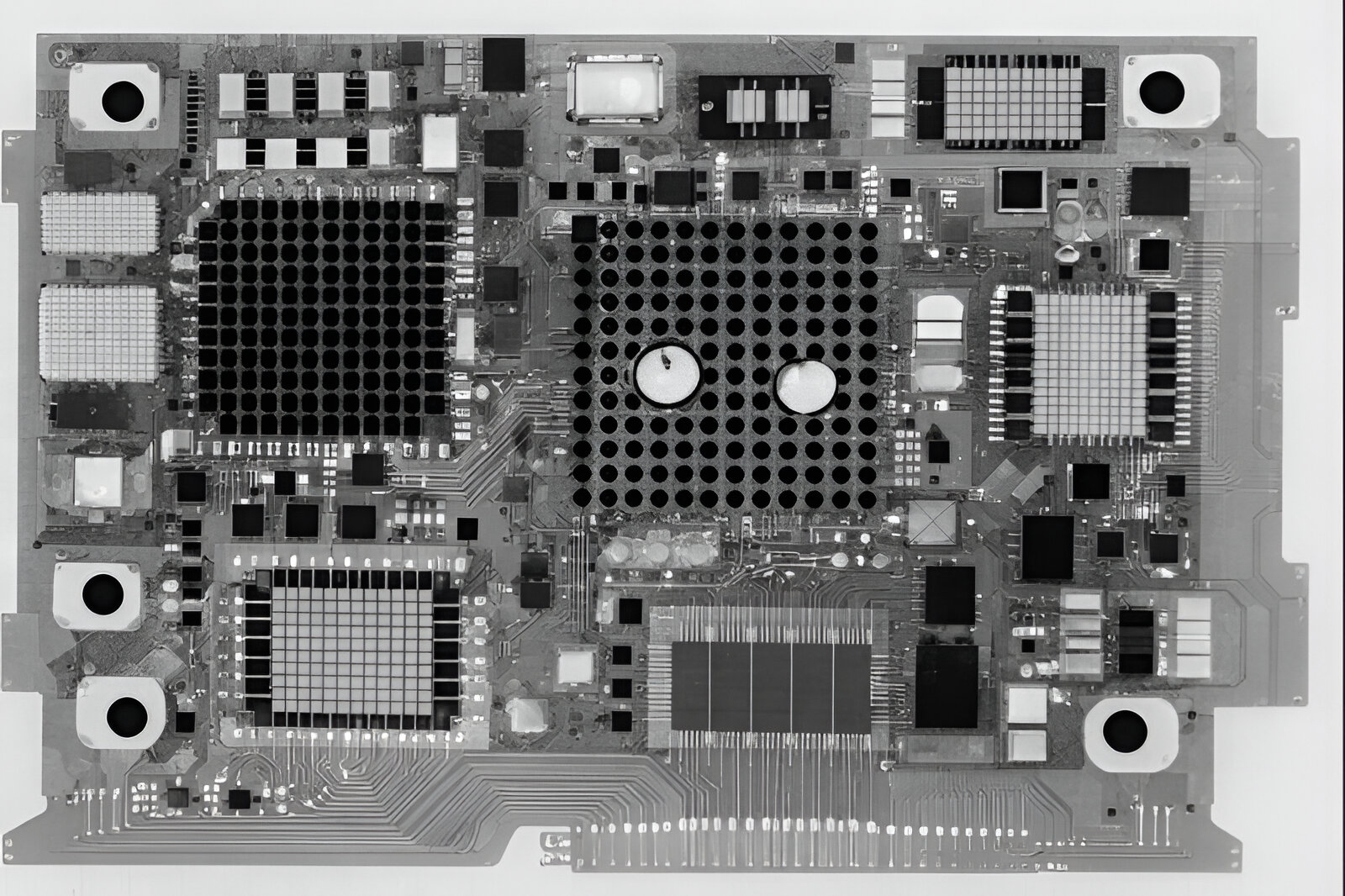
X-ray inspection uses high-energy radiation to penetrate materials and produce images of internal structures, ideal for opaque assemblies like printed circuit boards. In automotive applications, it targets hidden features such as ball grid array solder balls, via fills, and wire bonds that optical methods cannot access. This technique matters because automotive environments accelerate failure modes like solder joint cracking under thermal cycling or vibration-induced fatigue. Without thorough internal checks, latent defects escape detection, compromising system reliability.
The push for electrification and autonomy heightens stakes, with electronics handling power distribution and sensor fusion. X-ray inspection automotive directly addresses these by quantifying voiding or misalignment that could propagate under stress. Factory insights show it reduces escape defects by enabling 100% inspection of critical areas. For electric engineers, it bridges design intent with manufacturing reality, ensuring components meet operational demands.
Harsh environment testing reveals how initial quality influences endurance. Components passing x-ray scrutiny demonstrate better resilience in simulated conditions like rapid temperature swings. Automotive PCB inspection routines incorporate x-ray to align with class 3 requirements for high-reliability products. Ultimately, it safeguards against field failures that erode trust in vehicle performance.
Technical Principles of X-Ray Inspection
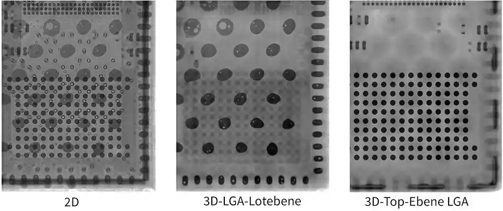
X-ray systems generate a beam from a source, typically a microfocus tube, which passes through the sample and strikes a detector to form a shadowgraph image. Density variations cause differential absorption, highlighting defects like voids as darker regions against solid solder. In 2D mode, transmission imaging suits quick solder joint checks, while 3D computed tomography reconstructs volumes for complex multilayer boards. Tilt and oblique angles enhance visibility of bridged joints or lifted balls in automotive assemblies.
Resolution depends on source spot size, typically under 5 microns for fine-pitch components, and magnification via object-to-detector distance. Automated systems use algorithms to measure void percentages or head-in-pillow defects automatically. Electric engineers appreciate how grayscale analysis distinguishes material contrasts, aiding precise defect classification. According to IPC-A-610, x-ray supports acceptability criteria for hidden solder joints by visualizing fillet formation and intermetallic growth.
Contrast enhancement and noise reduction via software improve interpretability in dense automotive boards. Radiation safety protocols limit exposure, ensuring operator protection during inline use. These principles enable detection of microcracks that initiate under vibration, critical for vehicle components. Integration with CAD data overlays nominal vs. actual geometries for variance analysis.
X-Ray Inspection for Vehicle Components in Harsh Environments
Automotive electronics face relentless stressors: thermal gradients from -40°C to over 150°C in power modules, constant road vibrations, and corrosive humidity. X-ray inspection for vehicle components detects precursors like incomplete reflow or delamination that worsen under these loads. Engine control units and battery management systems, with dense BGAs, benefit most from pre-stress x-ray to baseline integrity. Post-assembly scans confirm no shifts from handling or mounting.
Harsh environment testing protocols simulate lifecycles, but x-ray pre-qualifies boards for such abuse. Voids exceeding thresholds per IPC-7095 can trap gases, expanding under heat and cracking joints. Factory practices pair x-ray with thermal cycling to validate predictions. Electric engineers use these insights to refine solder paste recipes or reflow profiles for robustness.
Multilayer power PCBs in inverters demand volumetric x-ray to inspect buried vias and plane cracks. Vibration profiles per IEC 60068 correlate with x-ray findings on joint fillet adequacy. This targeted approach minimizes over-testing while maximizing coverage. Automotive electronics quality hinges on such layered verification.
Best Practices for Automotive PCB Inspection Using X-Ray
Implement x-ray at multiple stages: incoming components, post-reflow, and final assembly per J-STD-001 guidelines for soldered connections. Calibrate systems daily against phantoms mimicking solder densities for consistent grayscale. Train operators on automotive-specific artifacts like QFN paddle voids versus benign shrinkage. Automate where possible, programming regions of interest around critical ICs.
Integrate with AOI for hybrid flows, escalating optical flags to x-ray confirmation. Document thresholds aligned with class 3 criteria, tracking trends in void distribution across lots. For high-volume lines, inline oblique-angle cabinets handle throughput without halting production. Electric engineers should audit image archives against field returns for process correlation.
Combine x-ray with cross-sectioning on samples to validate interpretations. Firmware updates ensure compatibility with evolving component pitches down to 0.3mm. Supplier audits include x-ray mandates for outsourced assemblies. These practices elevate automotive PCB inspection to predictive quality control.

Challenges and Solutions in X-Ray Implementation
Interpreting dense automotive boards poses challenges, as overlapping features obscure defects. Solution: employ multi-angle acquisition and slicing software for layered views. Radiation dose accumulation risks sensitive devices, mitigated by low-kV protocols and shielding. Cost of high-end 3D systems demands ROI justification via defect escape reduction data.
Operator variability affects consistency; counter with standardized training and AI-assisted classification. Throughput limits in high-mix production resolve via dual-lane setups. Factory metrics show these adaptations cut false calls by focusing on high-risk zones like power QFNs. Electric engineers balance resolution needs with cycle time for scalable deployment.
Material variations, like lead-free solders, alter contrasts; recalibrate for alloy-specific profiles. Integration with MES systems logs results for traceability. Addressing these ensures x-ray delivers on harsh environment reliability promises.
Conclusion
X-ray inspection stands indispensable for automotive electronics quality, unveiling defects that threaten performance in demanding conditions. From BGA voids to via integrity, it enforces standards like IPC-A-610 and IPC-7095, guiding factory processes toward zero-escape goals. Electric engineers leverage its precision to predict field behavior under vibration and thermal stress. Adopting best practices integrates it seamlessly, enhancing overall automotive PCB inspection efficacy.
Prioritizing x-ray fortifies vehicle safety and longevity. As electronics densify, its role expands, demanding continual refinement. Reliable components start with invisible validations.
FAQs
Q1: What defects does x-ray inspection automotive detect in vehicle components?
A1: X-ray inspection automotive excels at identifying hidden solder issues like voids, bridges, and cracks in BGAs and QFNs, invisible to surface methods. It also reveals via fill inadequacies and wire bond breaks in multilayer boards. In harsh environment testing, these early detections prevent fatigue failures under vibration. Factory protocols per IPC standards use it for class 3 compliance, ensuring automotive electronics quality.
Q2: How does x-ray support harsh environment testing for automotive PCBs?
A2: Harsh environment testing simulates thermal cycling and shocks, where x-ray baselines joint integrity pre-stress. It quantifies voiding that expands under heat, correlating with IEC 60068 profiles. Post-test scans pinpoint degradation modes like microcracks. This iterative approach refines designs for endurance. Automotive PCB inspection routines integrate it to validate reliability margins.
Q3: When is x-ray inspection essential in automotive electronics quality control?
A3: X-ray becomes essential post-reflow for hidden joints and before encapsulation in ECUs or sensors. High-reliability demands mandate it for 100% coverage of critical arrays. J-STD-001 recommends it where visual access fails. Electric engineers apply it to troubleshoot escapes, bolstering x-ray inspection for vehicle components.
Q4: What are best practices for integrating x-ray in automotive PCB inspection?
A4: Calibrate systems for solder contrasts and automate ROI scans on power modules. Pair with AOI for efficiency and document per IPC-7095 void criteria. Train on automotive artifacts and track trends for process tweaks. This factory-driven method ensures robust automotive electronics quality in production.
References
IPC-A-610 — Acceptability of Electronic Assemblies. IPC, 2020
IPC-7095 — Design and Assembly Process Implementation for BGAs. IPC, 2018
J-STD-001 — Requirements for Soldered Electrical and Electronic Assemblies. IPC, 2020
IEC 60068 — Environmental Testing. IEC, 2017


