ALLPCB


Introduction
High-density interconnect (HDI) printed circuit boards enable compact electronics with superior performance, packing more functionality into smaller spaces through microvias, finer lines, and stacked layers. As electrical engineers transition designs from prototype to high-volume production, scaling HDI PCB manufacturing introduces complexities in process control, yield management, and cost efficiency. The HDI PCB manufacturing process demands precision at every stage, from laser-drilled vias to sequential lamination, to meet the demands of applications like smartphones, medical devices, and automotive systems. Challenges arise in assembly due to component density and thermal stresses, while quality control ensures reliability under IPC standards. Effective scaling requires optimizing workflows to balance performance, cost, and manufacturability. This article explores the journey from prototype validation to production ramp-up, providing factory-driven insights for engineers.
Understanding HDI PCBs and the Need for Scaling
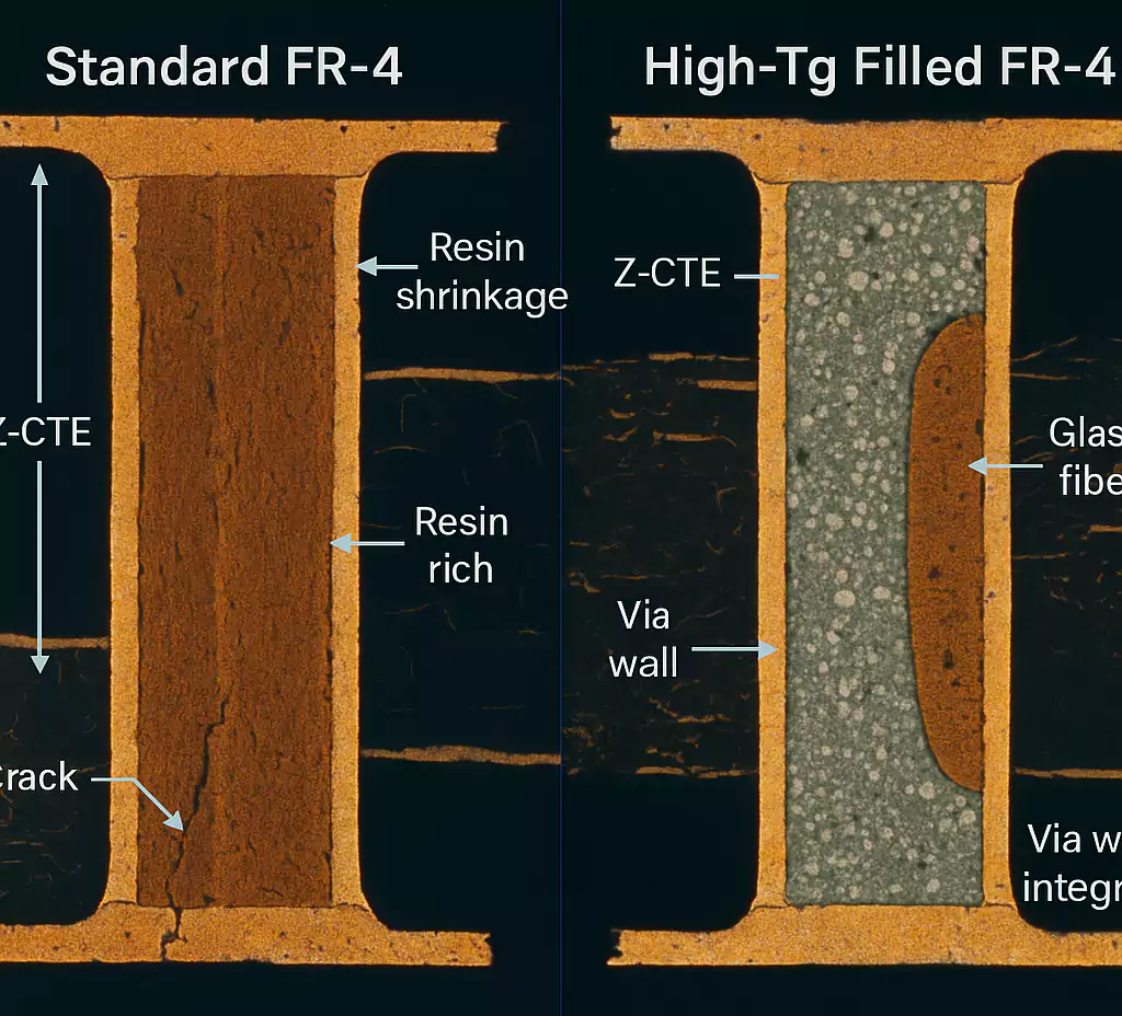
HDI PCBs feature higher wiring density per unit area compared to conventional boards, incorporating blind, buried, and microvias with diameters typically under 150 microns. These boards support advanced packaging like BGAs and CSPs, reducing signal path lengths for better electrical performance and lower power consumption. Prototyping HDI designs validates feasibility on small panels with flexible tolerances, but production scaling shifts to large panels for economy of scale. Factory experience shows that early prototype iterations often reveal issues like via reliability or layer alignment, which must be resolved before volume runs. Scaling matters because it amplifies small defects into major yield losses, impacting time-to-market and profitability. Engineers must anticipate these shifts to design for manufacturability from the outset.
The HDI PCB Manufacturing Process: Prototype Versus Production
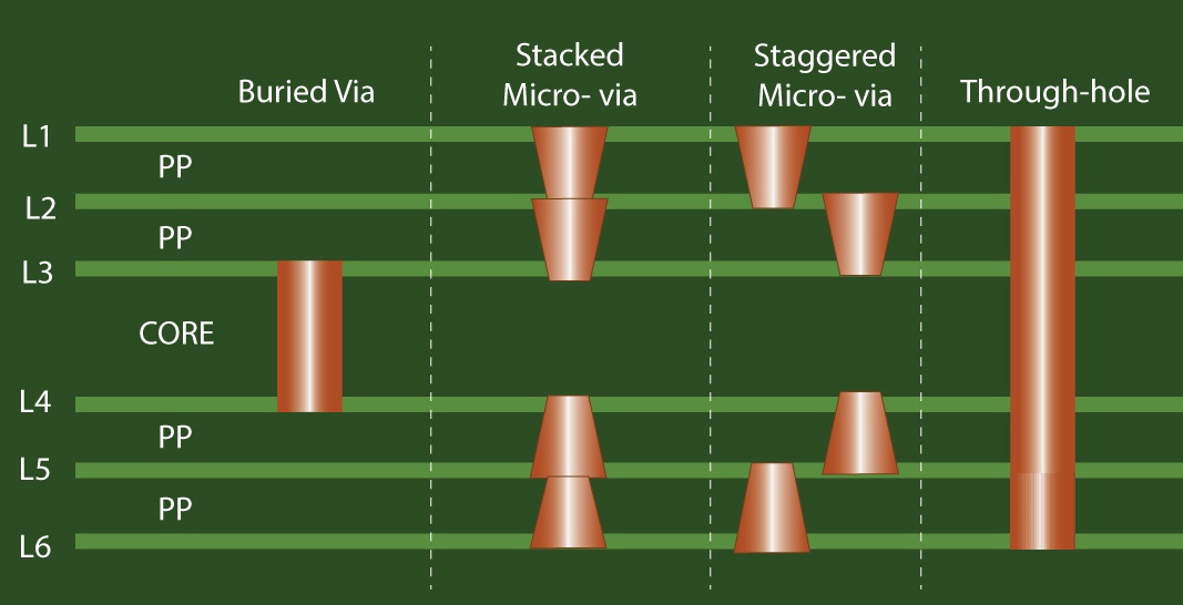
The HDI PCB manufacturing process begins with design transfer to photoplots and drill files, followed by material preparation using thin cores and prepregs suited for sequential build-up. Inner layers undergo imaging, etching, and black hole treatment to prevent smear during drilling. Laser ablation creates microvias, which are then filled with conductive epoxy or electroplated copper, enabling stacked or staggered configurations. Outer layers receive similar processing, with final plating, solder mask, and silkscreen application. In prototyping, single boards or small panels allow rapid turnaround with looser controls, but production employs multi-up panelization on 18x24 inch sheets to maximize throughput.
Scaling introduces rigorous process controls, such as automated optical inspection after each lamination cycle to detect misalignment. Factories optimize via fill methods to prevent voids, ensuring compliance with IPC-2226 design standards for high-density interconnects. Production lamination uses controlled pressure and temperature ramps to minimize warpage in multi-layer stacks. Electrical testing verifies continuity across thousands of nets, with flying probe for prototypes evolving to bed-of-nails for volume. Yield mapping from prototypes guides production adjustments, targeting over 95% first-pass yields through data analytics. This structured progression ensures HDI boards meet performance specs in real-world applications.
HDI PCB Assembly Challenges in Scaled Production
HDI PCB assembly challenges intensify with scaling due to ultra-fine pitches below 0.3mm and high component counts exceeding 1000 per board. Warpage from asymmetric lamination causes placement inaccuracies, leading to open joints or tombstoning during reflow. Microvias under BGAs demand precise solder paste deposition, as stencil apertures smaller than 0.2mm risk insufficient volume or bridging. Thermal management becomes critical, with CTE mismatches between dielectrics and components causing cracks under repeated cycling. Factories address these by implementing low-temperature solders and nitrogen reflow atmospheres to reduce oxidation.
Overcoming HDI PCB assembly challenges requires advanced equipment like 10-micron placement accuracy and jet printing for paste. Rework is labor-intensive, often needing laser soldering for BGA removal without damaging vias. Scaling demands statistical process control to monitor CpK values above 1.67 for key parameters. Collaboration between design and assembly teams early in prototyping mitigates issues like pad cratering from excessive pressure. Factories use simulation tools to predict warpage and adjust stack-ups accordingly. These practices ensure reliable assembly yields scale with volume.
HDI PCB Quality Control Measures for Production Reliability
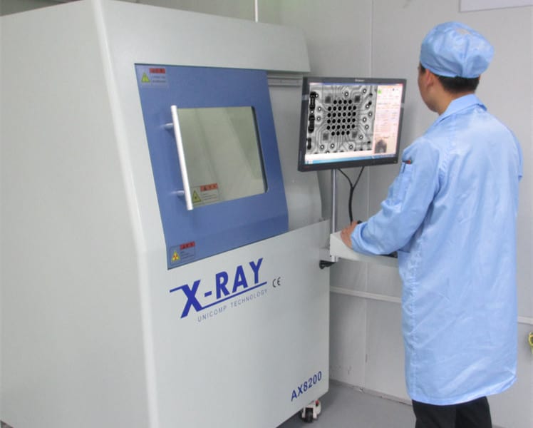
HDI PCB quality control spans in-process verification and final testing to detect defects invisible to the eye. Automated optical inspection (AOI) scans for trace defects post-etching, while X-ray examines via fill and BGA voids. Cross-sectioning samples validates layer registration and via quality per IPC-6016 specifications for HDI boards. Electrical testing confirms opens, shorts, and resistance, with functional tests simulating end-use conditions. Warpage measurement using shadow moire ensures boards stay within 0.75% tolerance for assembly.
In production, 100% inspection replaces sampling, with data traceability linking defects to process steps. IPC-A-600 acceptability criteria guide visual and dimensional checks, classifying boards as Class 2 or 3 based on application. Flying probe testers handle prototype complexity, transitioning to universal grids for high-volume. Environmental stress screening, like thermal cycling, uncovers latent weaknesses. Factories maintain cleanrooms to prevent contamination, critical for microvia integrity. Robust HDI PCB quality control sustains high yields and customer confidence.
Strategies for HDI PCB Cost Optimization
HDI PCB cost optimization starts with design choices like minimizing layer count and preferring staggered over stacked vias to reduce cycles. Panel utilization above 80% through efficient nesting cuts per-board expenses significantly. Selecting low-loss dielectrics with stable pricing balances performance and budget. Factories optimize sequential lamination by grouping build-ups, shortening throughput time from weeks to days.
Yield improvement drives savings, with root-cause analysis on prototypes preventing scrap in production. Standardizing via sizes and trace widths aligns with equipment capabilities, avoiding custom tooling fees. Volume commitments unlock material discounts and dedicated lines. HDI PCB cost optimization also involves supplier qualification for consistent via fill chemistry. Post-production, rework minimization through upfront DFM reviews pays dividends. Engineers achieve 20-30% reductions by iterating prototypes with cost models.
Best Practices for Seamless Scaling
Adopt design for manufacturing (DFM) reviews at prototype stage to flag scalability risks like excessive microvia density. Maintain material datasheets with consistent Tg and CTE for reliable lamination. Implement SPC across drilling, plating, and assembly for proactive adjustments. Partner with factories experienced in HDI classes 4-6 for capability matching. Document lessons from prototypes into production work instructions. These practices ensure smooth transitions and sustained quality.
Conclusion
Scaling HDI PCB manufacturing from prototype to production demands mastery of the HDI PCB manufacturing process, mitigation of assembly challenges, rigorous quality control, and strategic cost optimization. By leveraging standards like IPC-2226, IPC-6016, and IPC-A-600, engineers achieve reliable, economical high-volume output. Factory-driven insights emphasize early planning and data-driven refinements for success.
FAQs
Q1: What are the main steps in the HDI PCB manufacturing process?
A1: The HDI PCB manufacturing process includes inner layer etching, laser microvia drilling, via filling, sequential lamination, outer layer imaging, and final finishing. Prototypes focus on small-scale validation, while production scales with panelization and automated inspections. Compliance with IPC-6016 ensures via integrity and layer alignment. This structured approach minimizes defects and supports high yields.
Q2: What are common HDI PCB assembly challenges during scaling?
A2: HDI PCB assembly challenges include warpage-induced misalignment, fine-pitch soldering defects, and thermal stresses on microvias. High component density complicates placement and rework. Solutions involve precise stencils, nitrogen reflow, and warpage simulation. Factories use advanced pick-and-place systems for consistency. Early DFM resolves most issues before production.
Q3: How does HDI PCB quality control differ in production?
A3: HDI PCB quality control in production employs 100% AOI, X-ray for voids, and electrical testing versus prototype sampling. IPC-A-600 criteria classify acceptability, with cross-sections verifying microvias. Traceability links defects to processes for continuous improvement. This ensures Class 3 reliability at scale.
Q4: What strategies optimize HDI PCB cost in manufacturing?
A4: HDI PCB cost optimization involves panel efficiency, yield enhancement via SPC, and simplified stack-ups. Staggered vias reduce lamination cycles, while standard materials lower expenses. Prototype iterations with cost modeling guide production. Factories achieve savings through volume planning and defect prevention.