ALLPCB


Introduction
PCBA field failures disrupt operations, lead to costly recalls, and damage reputations in demanding applications like automotive and industrial electronics. These failures occur after deployment in real-world environments, often under thermal cycling, vibration, or humidity that accelerate wear. Electric engineers face the challenge of dissecting these issues to prevent recurrence. This guide outlines PCBA field failure analysis steps, from initial reporting to corrective actions, drawing on proven engineering practices. By following a systematic approach, teams can transform failures into opportunities for reliability improvements. Understanding root causes ensures long-term product robustness.
What Is PCBA Field Failure Analysis and Why It Matters
PCBA field failure analysis involves investigating assembled boards returned from customer sites to identify why they malfunctioned under operational stress. Unlike factory tests, field analysis accounts for uncontrolled variables like prolonged exposure to moisture or mechanical shocks. It matters because early failures erode trust and inflate warranty costs, while thorough analysis reveals design or process gaps. Engineers use this process to refine PCBA root cause analysis, enhancing overall system reliability. In high-stakes sectors, such investigations align with quality expectations and reduce downtime. Ultimately, effective analysis bridges the gap between lab validation and field performance.
Common Causes of PCBA Field Failures
Solder joint defects top the list of PCBA field failures, including cold joints from insufficient reflow or bridges causing shorts during vibration. Component misalignment during assembly leads to intermittent opens, exacerbated by thermal expansion mismatches. Environmental factors like humidity promote corrosion on exposed pads, forming conductive paths that trigger erratic behavior. Mechanical stresses from shocks fracture vias or delaminate layers, common in mobile devices. Contamination residues from flux trap moisture, accelerating dendritic growth over time. Thermal overloads degrade insulators, creating high-resistance paths that fail under load.
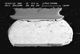
Overheating often stems from poor heat dissipation, where high-power components exceed material limits during extended operation. Electrostatic discharge during handling zaps sensitive ICs, manifesting as latent failures post-assembly. Plating voids in vias weaken interconnections, failing under cyclic loading. These causes highlight the need for multifaceted testing beyond initial production checks.
PCBA Field Failure Analysis Steps
PCBA field failure analysis steps begin with collecting detailed failure reports from the field, including symptoms, usage history, and environmental data. Returned units undergo preliminary sorting to group similar issues, prioritizing high-impact cases. Visual inspection follows, using stereomicroscopes to spot obvious defects like cracked components or burn marks. Non-destructive electrical tests, such as in-circuit probing, isolate shorts or opens without altering the board. Documentation at each stage tracks observations for traceability.
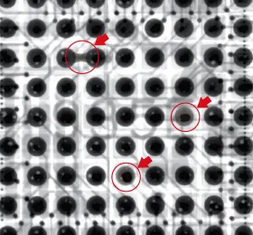
Next, advanced non-destructive methods like X-ray fluoroscopy reveal hidden voids in ball grid array solder balls or via misalignment. Thermal imaging identifies hot spots indicative of poor connections or overloaded traces. If needed, scanning acoustic microscopy detects delaminations or cracks internally. These steps comply with test methods in IPC-TM-650, ensuring standardized evaluation. Engineers log findings in a centralized database to correlate with production batches.
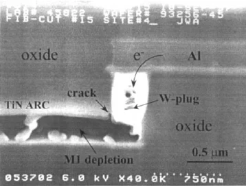
Destructive analysis proceeds only on confirmed samples, involving microsectioning to examine cross-sections for plating integrity or intermetallic formation. Chemical analysis via SEM/EDX quantifies contaminants contributing to corrosion. Each step builds evidence toward root cause confirmation. Finally, replicate failure conditions in lab simulations to validate findings. This structured progression minimizes guesswork and accelerates resolution.
PCBA Root Cause Analysis Techniques
PCBA root cause analysis starts with fault isolation, using functional testers to replicate field symptoms under controlled conditions. Tools like oscilloscopes capture intermittent signals, pinpointing timing-related issues. Fishbone diagrams categorize potential causes into materials, methods, machines, and environment for systematic review. Hypothesis testing recreates stressors, such as thermal cycling per IPC-TM-650 guidelines, to confirm mechanisms like fatigue cracking.
Failure Mode and Effects Analysis (FMEA) quantifies risks by scoring severity, occurrence, and detection, prioritizing actions for high-risk modes. For solder-related failures, dye-and-peel tests reveal non-wetting areas linked to surface oxidation. Acoustic imaging distinguishes voids from delaminations in multilayer boards. These techniques ensure causes like contamination or stress are not misattributed to symptoms.
In field contexts, correlate batch data with supplier lots to trace material variances. Iterative 5-Why questioning drills down from symptoms to process origins. Validation through accelerated life testing verifies root causes under exaggerated conditions. This depth prevents superficial fixes and fosters durable solutions.
PCBA Failure Reporting Best Practices
PCBA failure reporting captures essential details like failure mode, time-to-failure, and operating conditions in a standardized template. Include photos, electrical logs, and environmental notes from end-users for context. Use digital platforms to tag reports by batch, enabling trend analysis across units. Categorize failures as electrical, mechanical, or thermal to streamline triage.
Cross-reference reports with manufacturing records to spot patterns, such as spikes post-supplier change. Anonymize sensitive customer data while retaining traceability. Regular reviews disseminate insights via engineering bulletins, promoting team-wide learning. Adhering to ISO 9001 principles ensures reporting drives continuous improvement.
Share aggregated metrics in dashboards, tracking mean time between failures. This practice turns raw data into actionable intelligence for proactive interventions.
Developing PCBA Corrective Action Plans
PCBA corrective action plans stem from verified root causes, specifying immediate containment like quarantining affected batches. Short-term fixes include rework per IPC-A-610 acceptability criteria, such as reflowing suspect joints. Long-term measures target origins, like revising stencil designs for better paste release or qualifying alternate materials.
Implement process controls, such as enhanced bake-out before reflow to mitigate moisture. Supplier audits enforce incoming inspections for components prone to field issues. Track plan effectiveness through post-implementation monitoring and field return rates.
Verification involves retesting reworked units and accelerated simulations. Update design rules, like increasing via plating thickness for thermal resilience. Document plans with timelines, responsibilities, and success criteria aligned with ISO 9001 quality management. This closes the loop from failure to enhanced reliability.
Troubleshooting Insights for Field Returns
Consider a scenario where multiple units fail intermittently after months in humid environments. Initial visual checks reveal corrosion on connectors, but electrical tests show opens elsewhere. X-ray uncovers via cracks, traced to CTE mismatch via microsectioning. Root cause links to inadequate glass transition temperature in the laminate under cycling.
Corrective involved specifying higher Tg materials and adding strain-relief features. Field validation confirmed zero recurrences post-deployment. Such cases underscore replicating operational profiles early. Engineers should prioritize vibration fixtures matching end-use spectra.
Conclusion
Mastering PCBA field failure analysis steps transforms reactive firefighting into proactive engineering. From meticulous reporting to robust corrective action plans, each phase builds resilience against real-world stresses. Integrating PCBA root cause analysis techniques like FMEA and advanced imaging ensures accurate diagnostics. Adhering to standards elevates practices, minimizing future risks. Electric engineers equipped with these tools deliver products that endure. Commit to this process for sustained field performance.
FAQs
Q1: What are the primary PCBA field failure analysis steps?
A1: PCBA field failure analysis steps include data collection from reports, visual and non-destructive inspections like X-ray, electrical testing, destructive microsectioning if needed, root cause verification, and corrective planning. Start with symptom documentation to prioritize. Use tools like thermal imaging for heat-related issues. This sequence, guided by IPC-TM-650 methods, isolates faults efficiently. Follow up with replication tests for confirmation.
Q2: How do you conduct effective PCBA root cause analysis?
A2: PCBA root cause analysis employs fault isolation via functional tests, hypothesis building with diagrams, and validation through lab simulations. Techniques like SEM/EDX identify contaminants, while FMEA prioritizes risks. Correlate with production data for process links. Avoid symptom chasing by drilling to origins, such as material variances. Document for repeatability and prevention.
Q3: What should PCBA failure reporting include for engineers?
A3: PCBA failure reporting must detail symptoms, usage environment, photos, electrical signatures, and batch info. Use templates for consistency and trend spotting. Include replication attempts to aid triage. This supports PCBA root cause analysis by providing context. Aggregate data drives systemic improvements per quality standards.
Q4: How to create PCBA corrective action plans after analysis?
A4: PCBA corrective action plans outline containment, root cause fixes like process tweaks, and verification testing. Assign owners, timelines, and metrics like reduced return rates. Incorporate design changes, supplier quals, and monitoring. Align with ISO 9001 for auditability. Test efficacy in accelerated conditions before full rollout.
References
IPC-A-610 — Acceptability of Electronic Assemblies. IPC
IPC-TM-650 — Test Methods for Printed Boards. IPC
ISO 9001:2015 — Quality Management Systems. ISO, 2015
J-STD-001 — Requirements for Soldered Electrical and Electronic Assemblies. IPC