 ALLPCB


In the fast-paced world of electronics manufacturing, ensuring the reliability and longevity of your products is non-negotiable. One critical process that stands between you and potential product failures is electronic component burn-in testing. But what exactly is burn-in testing, and why is it so vital? Simply put, burn-in testing stresses electronic components under extreme conditions to identify early failures before they reach the market. This process is a cornerstone of quality control, helping manufacturers deliver dependable products and avoid costly recalls or customer dissatisfaction.
In this detailed guide, we’ll explore the importance of burn-in testing, dive into various component reliability testing methods, and explain how burn-in testing for component failure can save your production line from disaster. Whether you’re an engineer, a quality assurance specialist, or a business owner in the electronics industry, understanding this process can make a significant difference in your manufacturing success.
What Is Electronic Component Burn-In Testing?
Burn-in testing is a quality assurance method used to detect early failures in electronic components by subjecting them to accelerated stress conditions. These conditions often include elevated temperatures, high voltages, and extended operation times that mimic years of real-world use in just a few hours or days. The goal is to “weed out” defective parts that might fail prematurely, ensuring that only reliable components make it into the final product.
Think of burn-in testing as a rigorous boot camp for your electronics. Just as soldiers are tested under tough conditions to ensure they’re ready for battle, components are pushed to their limits to confirm they can handle the demands of everyday use. For example, a semiconductor might be tested at 125°C with a voltage of 5.5V (slightly above its rated 5V) for 48 hours to simulate stress over a 5-year lifespan. This process helps identify weak components that could fail due to manufacturing defects, material flaws, or design issues.
Why Burn-In Testing Is Crucial for Electronics Manufacturing
The electronics industry thrives on trust. Customers expect devices—whether smartphones, medical equipment, or automotive systems—to work flawlessly from day one. A single failure can damage a brand’s reputation and lead to financial losses. This is where burn-in testing plays a pivotal role. Let’s break down why it’s indispensable:
- Early Failure Detection: Burn-in testing targets the “infant mortality” phase of a component’s lifecycle, where most failures occur due to manufacturing defects. By catching these issues early, manufacturers can prevent defective products from reaching customers.
- Improved Product Reliability: Products that pass burn-in testing are more likely to perform consistently over their expected lifespan, building customer trust and loyalty.
- Cost Savings: Identifying and replacing faulty components during production is far cheaper than handling warranty claims or recalls after products are in the field.
- Compliance with Standards: Many industries, such as aerospace and medical, have strict reliability requirements. Burn-in testing ensures components meet these standards, avoiding legal or regulatory issues.
For instance, in the automotive sector, a failing sensor in a vehicle’s braking system could have catastrophic consequences. Burn-in testing ensures such critical components can withstand harsh conditions like temperature swings from -40°C to 85°C and constant vibration over years of use.
Common Component Reliability Testing Methods
Burn-in testing isn’t a one-size-fits-all process. Different components and applications require tailored approaches to ensure reliability. Below are some widely used component reliability testing methods that often incorporate burn-in techniques:
1. Static Burn-In Testing
In static burn-in testing, components are subjected to elevated temperatures and voltages without active operation. For example, a capacitor might be held at 105°C and 120% of its rated voltage for 24 hours. This method is effective for identifying issues like dielectric breakdown or material degradation in passive components.
2. Dynamic Burn-In Testing
Dynamic testing goes a step further by operating the component under stress conditions. A microcontroller, for instance, might run at full load with a clock speed of 100 MHz (its maximum rated speed) while exposed to 85°C for 72 hours. This simulates real-world usage and uncovers failures related to thermal stress or electrical overstress.
3. Temperature Cycling
While not strictly burn-in, temperature cycling is often combined with it to test a component’s resilience to thermal expansion and contraction. A power transistor might be cycled between -55°C and 125°C over 100 cycles to ensure it can handle rapid temperature changes without cracking or delaminating.
4. High-Temperature Operating Life (HTOL)
HTOL is a burn-in method specifically for active components like ICs and transistors. It involves operating the component at high temperatures (e.g., 125°C) and slightly elevated voltages for extended periods, such as 1000 hours, to predict long-term reliability. This method is common in industries where failure is not an option, such as aerospace.
How Burn-In Testing Prevents Component Failure
The primary goal of burn-in testing for component failure is to eliminate weak links in the production chain. Electronic components can fail for various reasons—manufacturing defects, poor material quality, or design flaws. Burn-in testing accelerates the aging process to expose these vulnerabilities before they cause problems in the field.
For example, a batch of resistors might have micro-cracks in their ceramic coating due to a production error. Under normal conditions, these cracks might not cause failure for months or years. However, during burn-in testing at 100°C for 48 hours, the thermal stress could widen the cracks, causing the resistor to fail. By catching this early, manufacturers can scrap or rework the defective batch, preventing costly failures in finished products.
Moreover, burn-in testing provides valuable data for improving designs and processes. If a specific type of capacitor consistently fails under high-voltage burn-in conditions, engineers can investigate whether the issue lies in the material, design, or manufacturing process, leading to better products in future iterations.
Key Benefits of Burn-In Testing in Electronics Manufacturing
Implementing burn-in testing offers several tangible benefits that directly impact the bottom line and customer satisfaction. Let’s explore these advantages in detail:
- Enhanced Product Lifespan: Components that survive burn-in are more likely to last through their intended operational life, reducing the need for repairs or replacements. For instance, a power supply unit tested at 50°C for 96 hours is less likely to fail prematurely in a server room environment.
- Reduced Field Failures: Field failures—when a product breaks down after reaching the customer—are expensive and damaging to reputation. Burn-in testing minimizes these incidents by ensuring only robust components are used.
- Better Customer Satisfaction: Reliable products lead to happy customers who are more likely to recommend your brand and make repeat purchases.
- Data for Continuous Improvement: Burn-in testing generates data on failure rates and patterns, which can be used to refine manufacturing processes or component selection. For example, if 5% of a batch of LEDs fail at 80°C after 24 hours, it might indicate a need for a different supplier or design tweak.
Challenges in Implementing Burn-In Testing
While burn-in testing is undeniably beneficial, it’s not without challenges. Manufacturers must balance the advantages with practical considerations to make the process cost-effective and efficient.
- Time and Cost: Burn-in testing can be time-consuming and expensive, especially for high-volume production. Running a 1000-hour HTOL test on thousands of components requires significant resources, including specialized equipment and energy costs.
- Risk of Over-Stressing: If not carefully calibrated, burn-in conditions can damage otherwise good components. For instance, testing a delicate sensor at excessively high voltages (e.g., 6V instead of its rated 3.3V) might cause permanent damage rather than identifying pre-existing flaws.
- Complexity in Test Design: Designing effective burn-in tests requires expertise to simulate real-world conditions accurately. A poorly designed test might miss critical failure modes or produce misleading results.
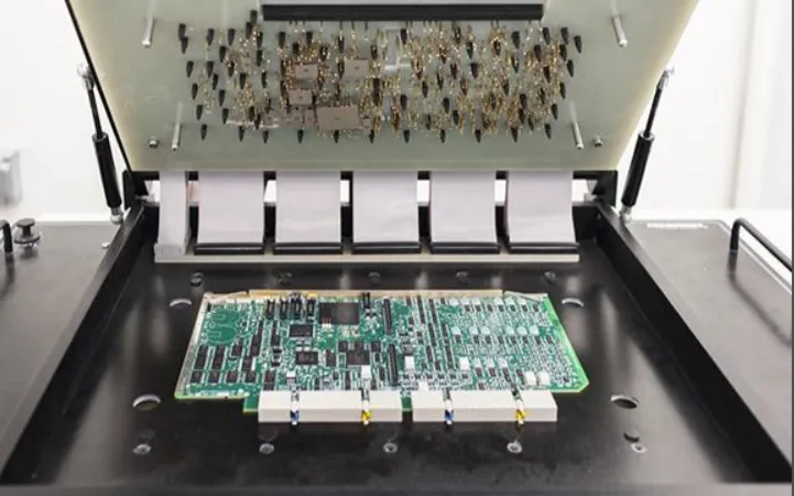
Despite these challenges, advancements in testing technology are making burn-in more accessible. Automated testing systems can now handle large batches of components simultaneously, reducing time and cost while maintaining accuracy.
Best Practices for Effective Burn-In Testing
To maximize the benefits of electronic component burn-in testing, manufacturers should follow these best practices:
- Tailor Tests to Components: Different components have different failure modes. Customize burn-in conditions based on the component type and its intended application. For example, a memory chip might require dynamic testing at 85°C, while a power diode might need static testing at 150°C.
- Use Realistic Stress Levels: Avoid over-stressing components to the point of artificial failure. Use manufacturer datasheets to determine safe limits for temperature and voltage, typically 10-20% above rated values.
- Monitor and Analyze Results: Track failure rates and patterns during burn-in to identify systemic issues in production or design. Use statistical tools to predict long-term reliability based on test data.
- Integrate with Other Testing: Combine burn-in with other reliability tests, like environmental stress screening or vibration testing, for a comprehensive quality check.
Future Trends in Burn-In Testing
As electronics become more complex and compact, burn-in testing methods are evolving to keep pace. Here are some emerging trends shaping the future of component reliability testing methods:
- Automation and AI: Automated burn-in systems integrated with artificial intelligence can optimize test parameters in real-time, reducing human error and improving efficiency. AI can also predict failure patterns based on historical data.
- Miniaturized Testing Equipment: With components shrinking in size, testing equipment is becoming more compact and precise, allowing for high-density testing of small-scale devices like wearables.
- Sustainability Focus: Energy-efficient burn-in systems are gaining traction as manufacturers aim to reduce the environmental impact of testing processes.
These innovations promise to make burn-in testing faster, cheaper, and more accurate, ensuring that even the most advanced electronics meet reliability standards.
Conclusion: Invest in Burn-In Testing for Long-Term Success
In the competitive world of electronics manufacturing, cutting corners on quality control is a recipe for disaster. Electronic component burn-in testing is not just a checkbox—it’s a strategic investment in your product’s reliability and your brand’s reputation. By identifying early failures, improving component lifespan, and reducing field issues, burn-in testing helps you deliver products that stand the test of time.
Whether you’re producing consumer gadgets, industrial equipment, or life-saving medical devices, integrating robust burn-in testing for component failure into your workflow is essential. With the right methods, equipment, and expertise, you can ensure that every component in your assembly meets the highest standards of performance and durability.
At ALLPCB, we understand the importance of reliability in every stage of electronics production. Our commitment to quality ensures that your projects benefit from cutting-edge testing and manufacturing processes. Ready to elevate your product reliability? Partner with us to build electronics that last.


