ALLPCB


Overview
Significant effort and progress have been made in developing biometric sensor technology that can reliably identify individuals. Available identification methods include fingerprint analysis, facial recognition, and unique iris-pattern identifiers. Engineers can combine a range of biometric ID technologies; other methods are still being developed, offering varying levels of authentication and a wide range of price points.
Biometric technology has advanced to the point that it is often unobtrusive in daily life. Many smartphones and tablets now use some form of biometric identification—typically fingerprint analysis—to control access and protect credit cards, bank accounts, and personal data.
Biometrics are rapidly replacing outdated employee identification systems that rely on traditional access cards. These cards have significant vulnerabilities, particularly when lost or stolen. As a result, offices, airports, and government agencies either implement redundant, resource-intensive access controls or leave critical areas exposed to fraud and unauthorized entry. Adding a biometric security layer to existing platforms can reduce fraud and substantially improve security.
After 9/11, the Department of Homeland Security spent over $100 million on biometric technology, and over an eight-year period the Department of Defense spent about $3.5 billion. For example, while attempting to distinguish insurgents from the public, the U.S. military collected millions of fingerprints, iris scans, and facial images from Iraqis and Afghans.
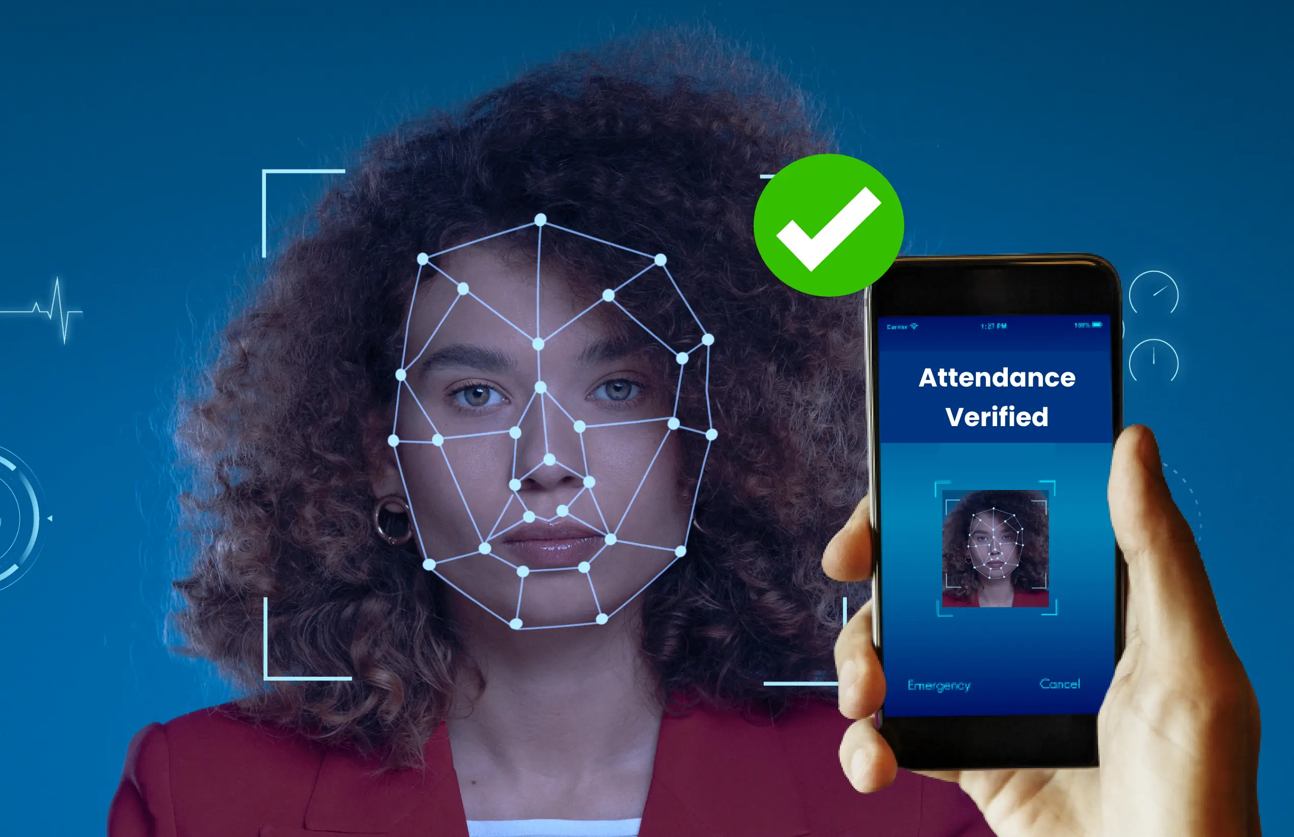
Modern biometric solutions are designed to work even under challenging conditions. For example, Facebook developed advanced facial recognition software that can identify individuals even when their faces are not fully visible. Once a person is tagged and entered into Facebook's system, the technology is reported to recognize them by body shape, hair, pose, posture, and clothing.
Similarly, a Mastercard implementation uses a selfie as the basis for authentication. Users take a selfie at purchase to authorize the transaction, confirming their identity and that they are the buyer. Users must blink when photographed to prevent hackers from using previously taken photos. The app also allows users to scan their fingerprint, confirming a second form of ID via Apple Pay.
Technology options
Omron's Human Vision Component (HVC) module demonstrates advances in underlying sensor technology. It is built on ten algorithms or functions, including face detection, face recognition, gender, age, expression, face pose, gaze and blink estimation, and hand and body detection. By comparing against faces registered in a database, the system can recognize people under various facial poses, expressions, and lighting conditions. The sensor can also estimate age and gender across different expressions and lighting. The HVC sensor even estimates facial expressions such as neutral, happy, sad, angry, and surprised.
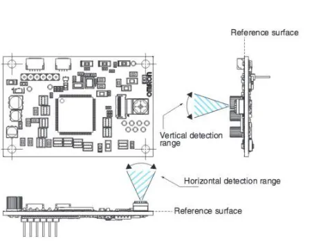
Figure 1: Image input specifications for horizontal and vertical detection ranges using the Omron B5T-01001(G) module.
Omron integrates its OKAO Vision image-sensing technology, camera, processor, and external interfaces onto a single 60 mm x 40 mm printed circuit board. The HVC acts as a sensor and provides data about detected persons via a UART interface. Beyond security applications, capturing this kind of data is useful whenever people interact with machines, from consumer devices to industrial environments.
To assist engineers, Omron also offers a demonstration kit for the human vision component called the B5T-001SG.
Pattern recognition hardware
Authentication commonly relies on pattern recognition. CogniMem Technologies' CM1K pattern-recognition chip is an example of this approach. The first ASIC version of the CogniMem neural network implemented 1,024 parallel neurons capable of learning and recognizing patterns up to 256 bytes in just a few microseconds. The neurons implement an associative memory that autonomously compares input patterns against stored reference patterns.
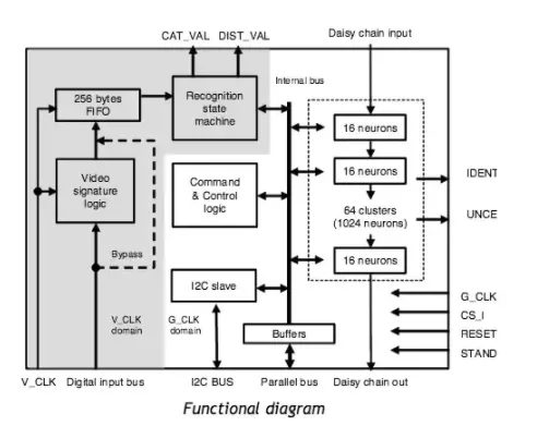
Figure 2: Functional block diagram of the CogniMem CM1K.
The chip supports two nonlinear classifiers that can categorize patterns even when data are ambiguous, events are unknown, or context and operating conditions change. Its low pin count and low power consumption make it suitable as a companion chip for smart sensors and cameras.
Features include the ability to identify one vector among 1,024 or any other number of vectors within 10 microseconds at a 27 MHz clock. Recognition time is independent of the number of models. The chip can learn a vector in 10 microseconds, save and load models (the knowledge base), and uses simple RTL instructions requiring fewer than a dozen registers. It offers parallel and serial communication and an optional digital input bus that connects directly to the recognition stage.
According to the vendor, the pattern-recognition approach is based on a simple architecture: a string of identical neurons running in parallel. During recognition, neurons engage in brief intercommunication for 15 clock cycles to find the best match. The CM1K also integrates a built-in recognition engine that receives vector data directly through a digital input bus, broadcasts it to the neurons, and returns the best-fit category after 3 microseconds. It can optionally extract a one-dimensional vector from two-dimensional video data.
Applications include assisted image recognition, signal recognition, and data-mining tasks. Image-recognition use cases include face recognition, gaze tracking, target tracking and identification, and object recognition. In signal recognition, it is used for speech recognition and related tasks. In data mining, uses include bioinformatics and fingerprint recognition.
Security hardware for fingerprints
Data security is as important as accurate verification in biometric applications. The MikroBUS Fingerprint click development board provides a click-board solution for adding biometric security to designs. The GTS-511E2 module is among the thinnest fingerprint sensors on the market and features a CMOS image sensor with a specialized lens and cover to capture real fingerprints and resist 2-D spoofing. It also includes an STM32 MCU for image processing.
The fingerprint click communicates with a host board MCU via UART (TX, RX) or SPI (CS, SCK, MISO, MOSI). It also includes a mini USB connector for connecting the click board to a PC. The vendor notes that a PC is often a more suitable platform for developing fingerprint-recognition software because of the processing required to compare inputs against large databases. The board also exposes additional GPIO pins for greater access to the onboard STM32. The fingerprint click is designed to run from a 3.3 V supply.
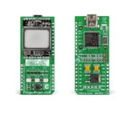
Figure 3: The MikroBUS fingerprint development system adds security to biometric applications.
Underlying algorithms
Algorithm development is critical for biometric applications. Broadly, algorithms fall into two groups: geometric and photometric. Geometric methods focus on distinguishing features, while photometric methods are statistical, converting an image into values and comparing those values against templates to reduce differences.
A recent trend is 3D face recognition, which uses 3D sensors to collect information about facial shape and to identify features such as eye-socket contours, the chin, and nose shape. This approach is less affected by lighting changes and can correctly recognize faces from various angles rather than relying on direct frontal images. Using 3D data points improves recognition accuracy.
Market outlook
With rapidly improving sensors, new highly integrated chips, and advanced algorithms, biometric security and identification are growing quickly. A Market & Markets report published in May projected the biometric systems market to reach $24.4 billion by 2020, with a compound annual growth rate of 17.9% from 2015 to 2020.