ALLPCB


Introduction
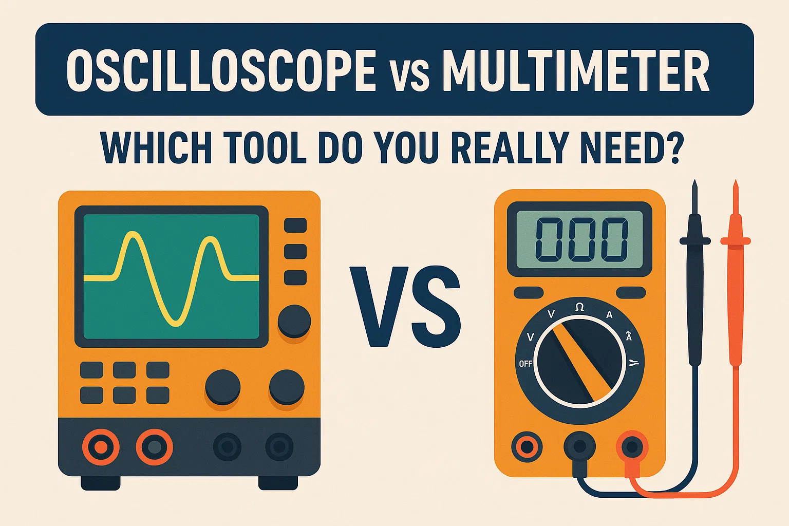
Printed circuit boards (PCBs) form the backbone of modern electronics, from consumer devices to industrial systems. While a multimeter excels at basic measurements like voltage, current, and resistance, it falls short in diagnosing complex faults in high-speed, multilayer boards. Intermittent issues, signal integrity problems, and thermal hotspots demand more sophisticated tools for accurate fault isolation. Electric engineers increasingly rely on advanced diagnostic equipment to reduce downtime and improve reliability in PCB repair and troubleshooting workflows. This article explores key tools beyond the multimeter, including oscilloscopes, thermal cameras, logic analyzers, in-circuit testing systems, and signal tracing methods. Mastering these enables precise diagnosis aligned with industry standards like IPC guidelines for board performance.
Limitations of Basic Tools and the Need for Advanced Diagnostics
Multimeters provide static readings essential for power rails and continuity checks, but PCBs today integrate high-frequency signals, mixed analog-digital circuits, and dense component layouts. Faults such as crosstalk, ground bounce, or solder joint cracks often manifest dynamically, evading simple DC tests. Advanced tools capture transient behaviors, visualize heat distribution, and probe internal nodes without full disassembly. For electric engineers, these instruments bridge the gap between symptom observation and root cause identification, enhancing efficiency in production testing and field repairs. Adopting them aligns with quality control practices outlined in IPC-6012E, which specifies performance criteria for rigid printed boards. Ultimately, investing time in these methods minimizes false positives and accelerates fault resolution.
Using Oscilloscopes for PCB Troubleshooting
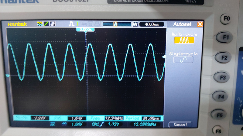
Oscilloscopes revolutionize PCB troubleshooting by displaying voltage waveforms over time, revealing anomalies like overshoot, ringing, or timing violations. Engineers probe signals at key nodes, such as clock lines or data buses, to assess rise times and jitter that multimeters cannot detect. High-bandwidth models with multiple channels allow simultaneous monitoring of related signals, aiding in crosstalk analysis between traces. Triggering functions isolate rare events, such as glitches from poor decoupling. In practice, start by verifying power supply ripple, then trace suspect signals from source to load, adjusting probe ground clips for minimal inductance. This technique proves invaluable for high-speed interfaces where signal integrity directly impacts system performance.
To apply oscilloscopes effectively, calibrate probes to 10x attenuation for accuracy and use math functions to compute differences between signals. Deselecting unnecessary channels reduces noise pickup, while persistence mode overlays multiple captures for statistical insight. Common pitfalls include probe loading effects, mitigated by low-capacitance probes, and ground loop issues, resolved with isolated inputs. For multilayer PCBs, access inner layers via test points or vias strategically placed during design. Integrating oscilloscope data with simulation models refines troubleshooting, ensuring compliance with signal quality metrics in JEDEC standards for component handling.
Thermal Imaging for PCB Repair
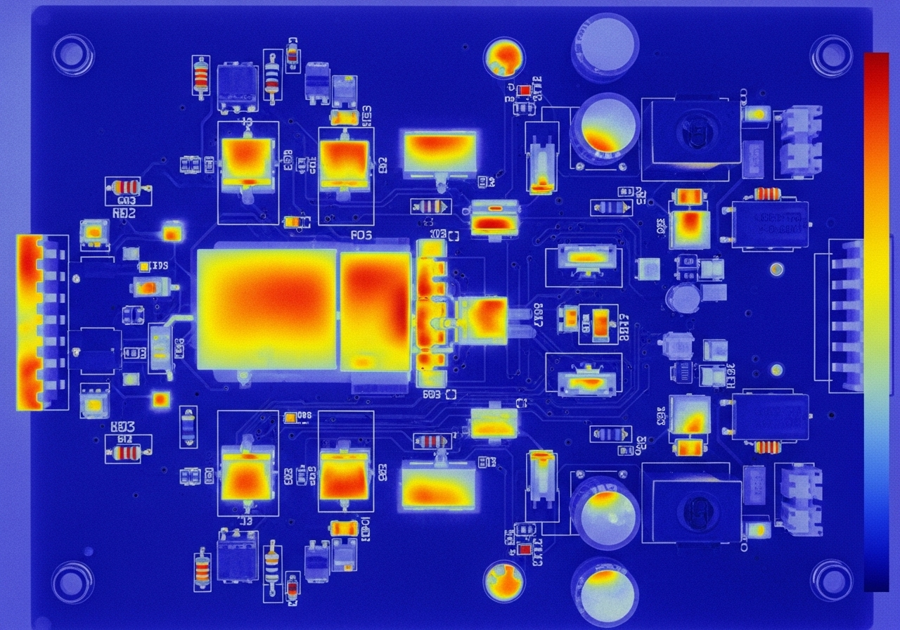
Thermal imaging cameras detect heat anomalies indicative of faults like shorted components, dry joints, or excessive power dissipation. Infrared sensors map surface temperatures, highlighting hotspots from current crowding or failing semiconductors. Unlike contact thermometers, they provide non-invasive, real-time views across the entire board, ideal for powered-up diagnostics. Engineers interpret thermograms by comparing hot spots against expected profiles from datasheet power ratings. Resolution and emissivity settings must match PCB materials, typically FR-4 with low emissivity requiring adjustments for accuracy. This method excels in identifying latent defects that escalate under load.
In PCB repair workflows, thermal imaging precedes invasive actions, guiding focused rework. Pair it with forced air cooling to provoke intermittent faults, then analyze cooling curves for capacitance loss clues. Software overlays annotate anomalies, facilitating team documentation. For high-reliability applications, correlate findings with IPC-A-600K acceptability criteria for solder joints, where excessive heat signals voids or cracks. Limitations include surface-only detection, so combine with X-ray for subsurface voids. Regular calibration against blackbody sources ensures measurement precision within 2 degrees Celsius.
Logic Analyzers for Digital Circuit Diagnosis
Logic analyzers capture and decode multiple digital signals simultaneously, essential for diagnosing state machines, protocols, and bus interactions in complex ASICs or FPGAs. They sample at gigasamples per second, storing deep histories for post-analysis with protocol decoders for I2C, SPI, or UART. Engineers set up state or timing modes: timing for edge relationships, state for qualified captures synced to a clock. This reveals setup/hold violations or glitches corrupting data integrity. Probes connect via clips or flying leads to fine-pitch pins, with buffering to handle capacitive loads.
Practical diagnosis begins with verifying clock stability, then correlating glitches to logic errors. Filtering reduces data volume, while correlators link analyzer traces to oscilloscope analog views. For embedded systems, scripting automates pattern searches, flagging protocol violations. In high-density boards, pod multiplexing expands channels. This tool shines in debugging firmware-hardware interactions, aligning with J-STD-001 requirements for soldered assembly integrity where poor connections mimic logic faults.
In-Circuit Testing (ICT) for PCB Fault Diagnosis
In-circuit testing (ICT) employs bed-of-nails fixtures to access hundreds of points, automating shorts, opens, component values, and parametric measurements. High-pin-count grids interface with flying probers or dedicated beds, executing programmed tests at vector rates exceeding 100 MHz. Digital guardians verify logic functionality, while analog sections measure passives and semiconductors in-circuit. Fault dictionaries isolate defects to specific nets, reducing manual probing. Setup involves CAD-derived fixture design, ensuring compliance with IPC-9252 guidelines for testability, though not repeating adjacent mentions.
Engineers optimize ICT by incorporating boundary scan for inaccessible nodes, minimizing fixture complexity. Parametric limits account for tolerances, with guarding techniques isolating nets from interactions. Post-test diagnostics refine algorithms based on field failures. For high-volume production, ICT throughput supports lean manufacturing, catching assembly defects early. Hybrid setups combine ICT with functional testing for comprehensive coverage.
Signal Tracing Techniques on PCBs
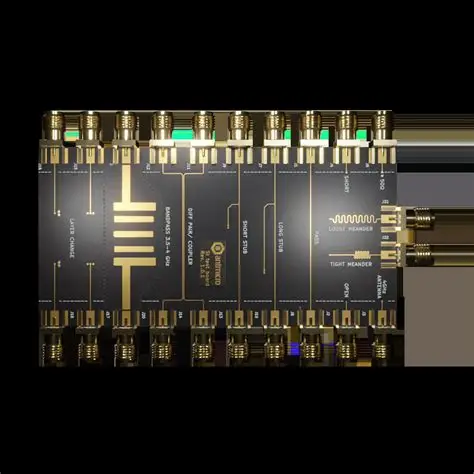
Signal tracing techniques systematically follow paths from input to output, combining tools for layered visibility. Visual inspection under magnification identifies mechanical damage, followed by continuity mapping with low-voltage sources. For buried signals, time-domain reflectometry (TDR) injects pulses to locate opens or stubs via impedance discontinuities. VNA-based methods characterize S-parameters for high-frequency traces. Layer-by-layer probing via exposed vias or edge connectors builds a signal integrity map.
Advanced tracing employs powered injection: stimulate inputs and monitor outputs with oscilloscopes or analyzers. Divide-and-conquer halves the board iteratively to pinpoint faults. Documentation via schematics with annotated traces aids repeatability. In multilayer designs, backdrilling test vias enhances access. These methods complement ICT, ensuring thorough coverage per IPC standards for board qualification.
Best Practices for Integrated PCB Fault Diagnosis
Integrate tools in a tiered approach: thermal imaging for quick scans, oscilloscopes for signals, analyzers for digital, ICT for production, and tracing for verification. Maintain a fault database correlating symptoms to tools, accelerating future diagnostics. Calibrate equipment regularly and train on artifact recognition, like thermal reflections or probe ringing. Collaborate across design, assembly, and test teams for proactive test point inclusion. Emphasize ESD protection during probing to avoid introducing faults. This holistic strategy upholds reliability standards, minimizing escapes to the field.
Conclusion
Advanced tools elevate PCB fault diagnosis beyond multimeter basics, enabling electric engineers to tackle dynamic, subtle issues in modern boards. Oscilloscopes, thermal imaging, logic analyzers, ICT, and signal tracing each offer unique insights, from waveform capture to automated net testing. Combining them systematically ensures faster root cause isolation and higher yield. Adhering to IPC and JEDEC standards reinforces these practices with proven benchmarks. As PCB complexity grows, proficiency in these tools remains a core competency for reliable electronics development.
FAQs
Q1: How do you use oscilloscopes for PCB troubleshooting intermittent faults?
A1: Oscilloscopes capture transient events using advanced triggering like edge, glitch, or runt detection. Set persistence mode to visualize rare occurrences over multiple acquisitions. Probe suspect nodes with short ground leads to minimize noise, and use infinite persistence for statistical analysis. This approach isolates timing issues in high-speed circuits effectively.
Q2: What role does thermal imaging play in PCB repair?
A2: Thermal imaging identifies overheating from shorts, high resistance joints, or failing passives by mapping infrared emissions. Power the board under load to provoke faults, then adjust emissivity for FR-4 accuracy. Hotspots guide targeted rework, preventing board-wide damage. Combine with electrical tests for confirmation in repair workflows.
Q3: When should logic analyzers be used for digital circuit diagnosis?
A3: Deploy logic analyzers for multi-bit bus decoding and protocol verification in microcontrollers or interfaces. Capture deep memory buffers to analyze long sequences, applying filters for relevant events. Sync with clocks for state reconstruction, revealing setup violations or corruption. Ideal for firmware debug where scopes lack bit-level detail.
Q4: How does in-circuit testing (ICT) detect PCB faults efficiently?
A4: ICT uses fixture probes for parallel net access, measuring continuity, values, and parameters rapidly. Fault isolation via dictionary lookup pinpoints defects without disassembly. Incorporate vector patterns for active components. Best for high-volume assembly verification, catching solder and placement errors early.
References
IPC-6012E — Qualification and Performance Specification for Rigid Printed Boards. IPC, 2017
IPC-A-600K — Acceptability of Printed Boards. IPC, 2020
JEDEC J-STD-001G — Requirements for Soldered Electrical and Electronic Assemblies. JEDEC, 2011