 ALLPCB


Introduction
Solderability remains a critical factor in printed circuit board assembly, directly influencing the reliability of electronic products. PCB plating and solderability determine how effectively molten solder bonds to copper surfaces during manufacturing processes. Poor solder wetting leads to defects such as incomplete joints or voids, compromising electrical performance and long-term durability. Engineers must prioritize surface finishes that preserve copper integrity while accommodating various assembly methods. This article explores best practices aligned with industry standards to achieve optimal results. Factory insights reveal that consistent plating control minimizes rework and enhances yield rates.
Understanding PCB Plating and Solderability
PCB plating refers to the protective surface finishes applied to exposed copper pads and traces after solder mask application. These finishes, such as hot air solder leveling, electroless nickel immersion gold, organic solderability preservative, immersion silver, and immersion tin, prevent oxidation and ensure reliable solder joints. Solderability describes the ability of a metal surface to form a strong metallurgical bond with molten solder through proper wetting. Effective PCB plating and solderability balance protection against environmental factors with compatibility for reflow or wave soldering. In high-volume production, selecting the right finish prevents issues like dewetting or solder beading. Standards like IPC J-STD-003 outline test methods to verify these properties before assembly.
Surface finishes vary in thickness uniformity and shelf life, impacting surface finish and solder joints formation. For instance, organic preservatives offer cost-effective protection but require careful handling to avoid degradation. Engineers evaluate finishes based on assembly type, component pitch, and end-use environment. Factory processes emphasize plating bath maintenance to achieve consistent coverage. Without proper plating, copper oxidizes rapidly, hindering solder flow during heating.
Technical Principles of Solder Wetting and Surface Finishes
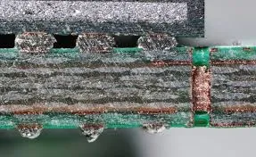
Solder wetting occurs when molten solder spreads across a clean metal surface, driven by surface tension and intermetallic compound formation. The process begins with flux activation, removing oxides and allowing solder to contact the base metal. Copper-solder intermetallics, such as Cu6Sn5, develop rapidly at the interface, strengthening the joint. Surface finishes modulate this reaction; thicker platings may delay wetting if not optimized. Poor surface finish and solder joints result from incomplete spreading, often visible as dewets or holidays. Understanding these mechanisms guides plating selection for specific thermal profiles.
Oxidation resistance defines finish performance over time. Exposure to humidity or temperature accelerates oxide growth on bare copper, reducing wettability. Immersion finishes like silver or tin dissolve into solder during reflow, exposing fresh copper for bonding. Nickel barriers in multilayer platings prevent diffusion but require precise thickness to avoid brittleness. Solder wetting balance tests measure zero-crossing time, where solder uptake equals drainage, indicating optimal flow. These principles align with qualification specs in IPC-6012, ensuring boards meet performance criteria.
Interfacial reactions evolve during prolonged exposure to elevated temperatures. Excessive heating promotes excessive intermetallic growth, leading to fragile joints prone to fatigue. Finishes must withstand steam aging or thermal shock without compromising solderability. Factory data shows that controlled plating parameters correlate with uniform wetting angles below 30 degrees for ideal joints. Engineers model these interactions using thermal profiles from reflow ovens. Balancing protection and reactivity optimizes surface finish and solder joints reliability.
Related Reading: Wave Soldering Flux: Selecting the Right Type for Optimal Wetting and Minimal Residue
Best Practices for PCB Plating and Solderability
Selecting the appropriate surface finish starts with assembly requirements and environmental exposure. For fine-pitch components, thinner finishes like immersion gold over nickel excel in reflow soldering due to flat topography. Wave soldering favors thicker, solderable coatings to handle contact with molten alloy. Always specify finish thickness tolerances during fabrication to ensure consistency. Compatibility with lead-free solders demands finishes resistant to tin whisker formation. Documenting these choices in design files prevents downstream issues.
Plating process control involves rigorous bath chemistry monitoring and agitation. Maintain pH, metal ion concentration, and accelerator levels to deposit uniform layers. Pre-plating cleaning removes residues that cause plating voids, directly affecting solder wetting. Post-plating inspections verify coverage using visual and microscopic methods. Implementing statistical process control tracks variations across panels. These steps, rooted in factory protocols, enhance PCB plating and solderability.
Solderability testing verifies finish integrity per J-STD-001 requirements for soldered assemblies. Common methods include dip-and-look for visual wetting assessment and wetting balance for quantitative data. Perform tests after simulated aging, such as vapor phase steam exposure, to mimic storage conditions. Acceptance criteria specify minimum coverage percentages and contact angles. Integrate testing at incoming inspection and final quality checks. Regular audits correlate test results with field performance.
Ensuring Solder Mask Compatibility with Plating
Solder mask application precedes final plating, requiring precise registration to expose pads fully. Mask materials must withstand plating bath chemistries without swelling or delamination. Incompatible masks lead to underplating or contamination, degrading solderability. Factory best practices include mask baking to remove volatiles before plating immersion. Verify mask adhesion through tape tests post-cure. Solder mask compatibility ensures clean pad definition for optimal plating adhesion.
Overhang or encroachment from solder mask can shadow pads, causing uneven finish deposition. Design rules specify minimum web widths between pads to support mask integrity during plating. Liquid photoimageable masks offer finer resolution for high-density boards. Post-plating, inspect for mask-finishing interactions like lifting. These considerations prevent defects at the mask-plating interface. Proper alignment enhances overall surface finish and solder joints quality.
Troubleshooting Common Solderability Issues
Non-wetting often stems from oxidized or contaminated surfaces despite plating. Flux residue buildup from previous processes hinders solder flow. Implement ultrasonic cleaning before assembly to restore wettability. Excessive plating thickness delays intermetallic formation, observable in cross-sections. Adjust bath parameters or select alternative finishes for chronic cases. Thermal profiling reveals profile mismatches causing dewetting.
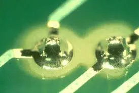
Bridging or icicles arise from poor solder mask compatibility or finish planarity. High-relief finishes promote solder draw to peaks. Optimize reflow ramp rates to control melt dynamics. Solder beading indicates incomplete wetting, tied to flux activity or humidity exposure. Storage in nitrogen-purged bags extends shelf life. Systematic root cause analysis, using solderability testing, resolves recurring defects.
Aging effects degrade organic finishes faster than metallic ones. Steam aging tests per IPC J-STD-003 predict long-term performance. Monitor humidity and temperature during shipping. Rework strategies involve light abrasion followed by fluxing, but prevention outperforms correction. Data logging from production lines identifies trends early.
Related Reading: PCB Plating Defects and How to Prevent Them
Conclusion
Achieving optimal solderability through PCB plating demands integrated design, process control, and verification. Prioritizing surface finish selection, rigorous testing, and solder mask compatibility yields reliable solder joints. Factory-driven practices aligned with standards like J-STD-001 minimize defects and support high-volume output. Engineers benefit from documenting specifications and collaborating with fabricators. Consistent application of these best practices ensures robust surface finish and solder joints in demanding applications. Future advancements in plating technologies will further enhance performance.
FAQs
Q1: What factors most influence PCB plating and solderability?
A1: Surface cleanliness, finish type, and storage conditions primarily affect solderability. Oxidation from exposure reduces wetting, while proper plating thickness ensures uniform solder flow. Testing per IPC J-STD-003 confirms compliance before assembly. Factory controls like bath monitoring prevent variations.
Q2: How does surface finish impact solder wetting during reflow?
A2: Surface finishes protect copper and facilitate solder spreading by minimizing oxides. Immersion finishes dissolve to expose base metal, promoting intermetallics. Uneven topography can cause incomplete wetting balance. Optimize profiles for consistent surface finish and solder joints.
Q3: Why is solderability testing essential for PCB quality?
A3: Solderability testing identifies potential assembly failures early, using methods like dip-and-look. It verifies plating integrity after aging simulations. Standards define acceptance for reliable joints. Integrating tests reduces rework in production.
Q4: How to ensure solder mask compatibility with PCB plating?
A4: Select masks resistant to plating chemistries and bake thoroughly before immersion. Maintain precise pad exposure to avoid shadowing. Inspect for adhesion post-process. This prevents contamination affecting solder wetting.
References
IPC J-STD-003D — Solderability Tests for Printed Boards. IPC, 2024
J-STD-001H — Requirements for Soldered Electrical and Electronic Assemblies. IPC, 2020
IPC-6012E — Qualification and Performance Specification for Rigid Printed Boards. IPC, 2017


