 ALLPCB


The electronics industry faces mounting pressure from electronic waste accumulation. Engineers increasingly explore fully biodegradable electronics as a pathway to reduce long-term environmental impact. These devices incorporate materials that break down naturally after their intended service life. Research focuses on substrates, conductors, and components that degrade into benign byproducts under composting or soil conditions. This approach aligns with broader sustainability goals in electrical engineering without compromising core functionality during operation.
Why Fully Biodegradable Electronics Matter
Fully biodegradable electronics represent devices built from materials capable of complete decomposition in natural environments. Substrates often derive from cellulose or similar biopolymers, while conductors may use metals such as magnesium that oxidize over time. The concept addresses the limitations of conventional printed circuit boards that persist in landfills for decades. Industry relevance stems from regulatory trends favoring reduced waste and resource recovery. Engineers in design and manufacturing evaluate these options for applications where device lifespan is intentionally limited, such as environmental sensors or single-use medical monitors.
Adoption requires balancing performance with end-of-life behavior. Traditional materials provide superior conductivity and thermal stability, yet biodegradable alternatives introduce trade-offs in mechanical strength and moisture resistance. Practical deployment demands careful material pairing to maintain electrical integrity until degradation begins. Standards play a supporting role in defining acceptable performance thresholds during the operational phase.
Technical Principles of Biodegradable PCB Design
Biodegradable PCB design centers on selecting substrates that support circuit patterning while enabling controlled breakdown. Cellulose-based materials offer a renewable foundation that can be processed into thin, flexible sheets suitable for circuit deposition. Conductive traces typically employ transient metals or organic compounds that lose functionality predictably when exposed to moisture or microbes. Dielectrics and encapsulants must protect active elements during use yet permit eventual dissolution or fragmentation.
Degradation mechanisms vary by material chemistry. Hydrolysis and enzymatic action drive breakdown in many biopolymers, with rates influenced by temperature, humidity, and pH. Engineers model these processes to ensure the device remains reliable for its target duration, often measured in weeks or months rather than years. Thermal and electrical properties of these materials generally fall short of conventional laminates, requiring design adjustments such as increased trace widths or additional protective layers during the functional period.
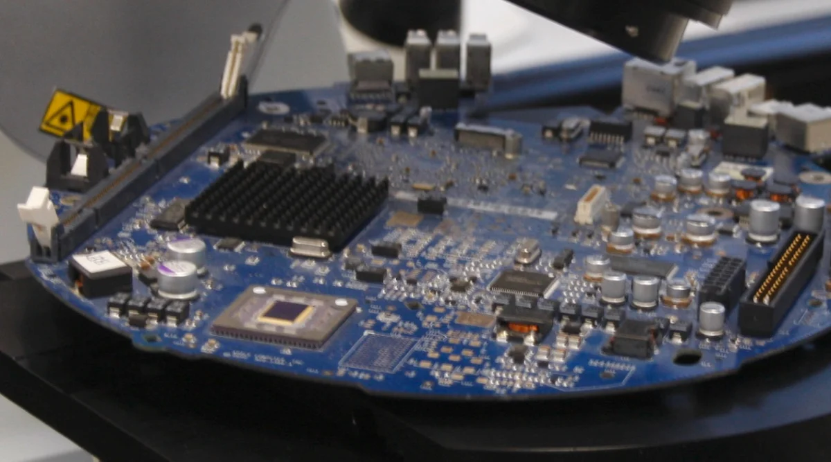
Component integration follows similar logic. Resistors and capacitors built from biodegradable composites must match the substrate's degradation timeline. Assembly techniques adapt conventional methods, with attention to avoiding permanent bonds that hinder composting. Performance validation includes accelerated aging tests to confirm stability before degradation initiates.
Practical Solutions and Best Practices in Design
Engineers begin by defining the required operational window and environmental exposure conditions. Material selection then proceeds iteratively, pairing a primary substrate with compatible conductors and dielectrics. Layering strategies often incorporate thin barrier coatings that delay moisture ingress until the device reaches end of life. Testing protocols evaluate both electrical performance and degradation behavior under standardized conditions.
Design rules emphasize simplicity to minimize interfaces that could impede breakdown. Single-layer or low-layer-count constructions reduce complexity compared with multilayer rigid boards. Trace geometries account for the lower conductivity of many biodegradable conductors, resulting in wider paths or alternative routing to maintain signal integrity. Thermal management relies on material properties rather than high-conductivity metals, influencing component placement and heat-spreading features.
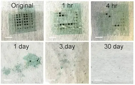
Quality considerations draw from established frameworks. Designs align with performance expectations outlined in relevant specifications for printed boards during the active phase. Environmental management practices support overall process sustainability. Prototyping involves small-batch fabrication followed by composting trials to verify complete material breakdown without harmful residues.
Collaboration across design, materials science, and testing teams accelerates iteration. Simulation tools predict both electrical behavior and degradation kinetics, reducing physical trial counts. Documentation captures material sources, processing parameters, and expected decomposition pathways for traceability.
Conclusion
Designing fully biodegradable electronics requires integrating material science with conventional electrical engineering principles. Success depends on selecting compatible components that deliver required performance while ensuring predictable end-of-life behavior. Structured approaches to material pairing, protective layering, and validation testing provide reliable pathways forward. Continued refinement of these methods supports broader industry movement toward reduced persistent waste.
FAQs
Q1: What defines fully biodegradable electronics in PCB design?
A1: Fully biodegradable electronics incorporate substrates, conductors, and components that decompose completely into non-toxic substances under composting or natural soil conditions. This approach targets applications with defined service lives, distinguishing them from conventional boards that resist degradation. Engineers focus on matching degradation rates across all elements to avoid partial remnants.
Q2: How does biodegradable PCB design address performance challenges?
A2: Biodegradable PCB design compensates for lower conductivity and thermal stability through adjusted trace dimensions, protective coatings, and simplified layouts. Material selection prioritizes compatibility between substrate and active elements to maintain functionality until the intended breakdown phase. Validation testing confirms both operational reliability and eventual compostability.
Q3: What role do industry standards play in compostable electronic components?
A3: Industry standards guide qualification of performance during the operational period and support consistent evaluation of environmental aspects. Specifications such as those from IPC help define acceptable electrical and mechanical properties, while environmental frameworks encourage sustainable practices throughout development. These references ensure designs meet baseline expectations without prescribing specific biodegradable materials.
Q4: How can engineers ensure controlled degradation in biodegradable electronics?
A4: Engineers ensure controlled degradation by modeling environmental triggers such as moisture and temperature, then selecting material combinations that respond predictably after the functional window. Barrier layers and encapsulation timing protect circuits during use. Post-use composting trials verify that all components break down without leaving persistent fragments.
References
IPC-6012E — Qualification and Performance Specification for Rigid Printed Boards. IPC, 2017
ISO 14001:2015 — Environmental Management Systems. ISO, 2015
ASTM D6400 — Standard Specification for Labeling of Plastics Designed to be Aerobically Composted in Municipal or Industrial Facilities. ASTM International, 2019





