 ALLPCB


Transporting printed circuit boards (PCBs) and electronic kits safely and sustainably is a growing concern for hobbyists, engineers, and manufacturers alike. Whether you're shipping a single DIY project or bulk orders for a business, ensuring your PCBs arrive undamaged while minimizing environmental impact is crucial. In this guide, we’ll explore the best practices for PCB board safe sustainable transport, offer tips for PCB electronic kit transport, and show you how to create greener shipping kits with a focus on board eco-responsibility DIY solutions.
This comprehensive blog post will walk you through the challenges of transporting delicate electronic components, eco-friendly packaging options, and actionable steps to balance safety with sustainability. Let’s dive into the details of protecting your PCBs while reducing your carbon footprint.
Why Safe and Sustainable PCB Transportation Matters
PCBs are the backbone of modern electronics, from smartphones to industrial machinery. These delicate components are highly sensitive to physical damage, static electricity, and environmental factors like moisture and temperature. A single crack or short circuit during transport can render a PCB useless, leading to costly replacements and delays. At the same time, the electronics industry faces increasing pressure to adopt sustainable practices, as traditional packaging materials like plastic and non-recyclable foam contribute to environmental waste.
By focusing on safe and sustainable transportation methods, you not only protect your investment but also contribute to a greener future. Sustainable shipping reduces waste, lowers carbon emissions, and aligns with global efforts to combat climate change. For DIY enthusiasts and small businesses, adopting eco-friendly practices can also enhance your reputation among environmentally conscious customers.
Key Challenges in PCB Electronic Kit Transport
Transporting PCBs and electronic kits comes with several challenges. Understanding these issues is the first step to overcoming them with effective solutions.
- Physical Damage: PCBs are fragile and can crack or bend under pressure. Components soldered onto the board can also break off during rough handling.
- Electrostatic Discharge (ESD): Static electricity can damage sensitive electronic components. Without proper protection, a small static shock during transport can fry a circuit.
- Environmental Factors: Exposure to moisture, extreme temperatures, or dust can corrode or short-circuit PCBs, especially during long-distance shipping.
- Environmental Impact: Traditional packaging materials like bubble wrap and plastic bags are often non-recyclable, contributing to landfill waste and pollution.
Addressing these challenges requires a combination of protective packaging and sustainable materials. Let’s explore how to tackle each issue while keeping eco-responsibility in mind.
Best Practices for Safe PCB Board Transport
To ensure your PCBs arrive in perfect condition, follow these best practices for safe transportation. These tips are designed for both DIY hobbyists and professionals handling bulk shipments.
1. Use ESD-Safe Packaging
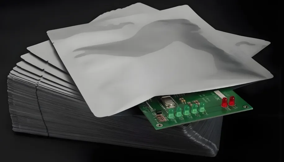
Electrostatic discharge is a major risk for electronic components. Always use ESD-safe materials, such as anti-static bags or foam, to protect your PCBs. These materials prevent the buildup of static electricity, safeguarding delicate circuits. For added protection, store PCBs in conductive containers or wrap them in aluminum foil before placing them in an anti-static bag.
2. Cushion Against Physical Shock
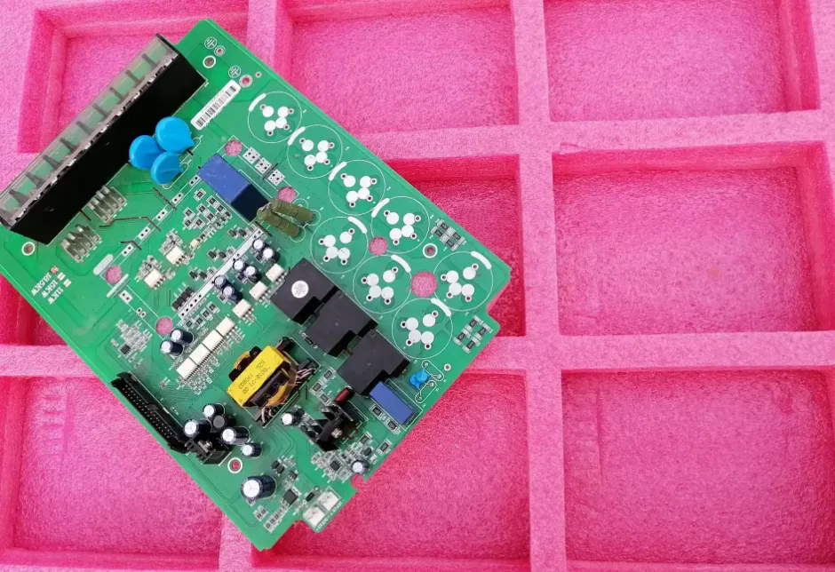
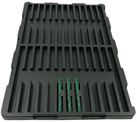
Physical damage can occur during transit due to drops or vibrations. Use cushioning materials like foam inserts or corrugated cardboard to absorb shocks. Place PCBs in a rigid box with at least 2 inches of padding on all sides to minimize movement. For electronic kits with multiple components, consider using compartmentalized boxes to keep parts separate and secure.
3. Protect from Environmental Hazards
Moisture and temperature fluctuations can wreak havoc on PCBs. Seal your components in moisture-resistant bags with desiccant packets to absorb any humidity. If shipping to extreme climates, use insulated packaging to maintain a stable temperature. Label packages with warnings like “Fragile” or “Keep Dry” to alert handlers to special care requirements.
How to Create Greener Shipping Kits for PCBs
Sustainability doesn’t mean sacrificing safety. With the right materials and methods, you can create greener shipping kits that protect your PCBs while reducing environmental impact. Here are some eco-friendly strategies to consider.
1. Opt for Recyclable and Biodegradable Materials
Replace plastic bubble wrap with biodegradable alternatives like cornstarch-based packing peanuts or recycled paper padding. Use cardboard boxes made from post-consumer recycled content instead of virgin materials. These options are just as effective at protecting your PCBs and can be recycled or composted after use.
According to recent studies, packaging waste accounts for a significant portion of landfill contributions globally. By switching to recyclable materials, you can reduce your waste footprint by up to 30%, depending on the materials used.
2. Minimize Packaging Size
Over-packaging not only wastes materials but also increases shipping costs and carbon emissions due to added weight and volume. Design your shipping kits to fit snugly around the PCB or electronic kit, minimizing empty space. This approach reduces the amount of material needed and lowers the environmental impact of transportation.
3. Partner with Eco-Friendly Shipping Services
Choose shipping carriers that prioritize sustainability, such as those using electric vehicles or carbon offset programs. Some carriers offer consolidated shipping options, which combine multiple packages into a single delivery route, reducing fuel consumption and emissions. Researching carrier practices can help align your PCB board safe sustainable transport efforts with broader environmental goals.
Board Eco-Responsibility DIY: Sustainable Solutions for Hobbyists
For DIY enthusiasts, adopting board eco-responsibility DIY practices is both achievable and rewarding. You don’t need large budgets or industrial resources to make a difference. Here are some practical ideas for sustainable PCB transportation on a smaller scale.
1. Reuse Packaging Materials
Before buying new packaging, look around for materials you can reuse. Old cardboard boxes, packing paper, or even fabric scraps can serve as cushioning for your PCBs. Reusing materials not only saves money but also prevents unnecessary waste from entering landfills.
2. Craft Custom Protective Cases
If you’re handy, consider creating custom protective cases for your electronic kits using sustainable materials like wood or recycled plastic. A simple wooden box lined with foam or felt can provide excellent protection for PCBs while being reusable for multiple shipments. Add a personal touch by designing the case to fit your specific project needs.
3. Educate Yourself on Local Recycling Programs
Learn about recycling options in your area for packaging materials and electronic waste. Many communities offer programs for recycling cardboard, paper, and even certain plastics. By properly disposing of or recycling materials, you ensure that your PCB electronic kit transport efforts don’t contribute to environmental harm.
Balancing Cost and Sustainability in PCB Shipping
One common concern is that sustainable practices might increase costs. While eco-friendly materials can sometimes be pricier upfront, they often lead to long-term savings and benefits. For instance, using durable, reusable packaging reduces the need for frequent replacements. Additionally, minimizing packaging size lowers shipping fees, as carriers often charge based on weight and dimensions.
To balance cost and sustainability, start small by incorporating one or two eco-friendly changes, such as switching to recycled cardboard or reusing materials. Track the impact on your budget and adjust as needed. Over time, these small shifts can add up to significant savings and a reduced environmental footprint.
Industry Trends in Sustainable PCB Manufacturing and Transport
The electronics industry is increasingly prioritizing sustainability, and this extends to PCB manufacturing and transportation. Innovations in green PCB production, such as using alternative substrate materials like polylactic acid (PLA) composites or recycled polyethylene terephthalate (PET), are gaining traction. These materials reduce the environmental impact of PCB production by up to 14% in terms of global warming potential, based on lifecycle assessments from recent studies.
Transportation practices are also evolving. Companies are exploring additive manufacturing techniques to reduce waste during PCB production, which in turn affects how products are packaged and shipped. Staying informed about these trends can help you adopt cutting-edge practices for PCB board safe sustainable transport.
Step-by-Step Guide to Preparing Your PCB for Sustainable Shipping
To wrap up, here’s a practical, step-by-step guide to preparing your PCB or electronic kit for safe and sustainable shipping. Follow these steps to ensure your components arrive intact while minimizing environmental impact.
- Assess Your Needs: Determine the size, weight, and fragility of your PCB or kit. This will guide your choice of packaging materials.
- Choose ESD Protection: Place the PCB in an anti-static bag or wrap it in conductive material to prevent static damage.
- Add Cushioning: Use eco-friendly padding like recycled paper or biodegradable foam to protect against shocks. Ensure at least 2 inches of cushioning on all sides.
- Seal Against Moisture: Include desiccant packets and seal the package in a moisture-resistant bag if shipping through humid areas.
- Select a Sustainable Box: Use a sturdy, recyclable cardboard box that fits snugly around the contents to avoid over-packaging.
- Label Clearly: Mark the package as “Fragile” and include handling instructions to alert carriers to the delicate contents.
- Partner with Green Carriers: Opt for a shipping service with sustainable practices, such as carbon-neutral delivery options.
By following these steps, you’ll ensure both the safety of your PCB and a reduced environmental impact during transport.
Conclusion: Building a Greener Future with Safe PCB Transport
Safe and sustainable transportation of PCBs and electronic kits is not just a trend—it’s a responsibility. By adopting best practices for PCB board safe sustainable transport and focusing on board eco-responsibility DIY solutions, you can protect your valuable components while contributing to a healthier planet. From using ESD-safe materials to choosing recyclable packaging and partnering with eco-friendly carriers, every step counts.
Whether you’re a hobbyist shipping a single project or a business handling bulk orders, these strategies for PCB electronic kit transport and creating greener shipping kits are within reach. Start small, stay informed about industry trends, and commit to making a difference. Together, we can build a future where electronics and sustainability go hand in hand.


