 ALLPCB


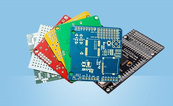
PCB solder mask is one of the most critical elements in the PCB manufacturing process. A deep understanding of solder mask materials, processes, and applications helps engineers design PCBs with superior performance, reliability, and efficiency. In this comprehensive guide, we will explore the composition, standards, application techniques, design considerations, and emerging innovations related to PCB solder masks—integrating related subtopics to provide a complete knowledge hub.
Composition of PCB solder mask
The formulation of PCB solder mask ink is fundamental to its effectiveness. It typically consists of the following components:
1. Resin
- Resin is the basic component of PCB solder mask, which determines the basic performance of the ink.
- Common types of resins include epoxy resin, acrylic resin, polyester resin, etc.
2. Pigment
- Pigments give PCB solder mask a specific color. Common colors include green, blue, black, white, etc.
- The choice of pigment not only affects the appearance of the PCB, but also is related to the light reflectivity and thermal stability of the solder mask layer. At the same time, it will also affect the manufacturing cost to a certain extent.
- Green is the most common solder mask color because it is visually comfortable and has a moderate reflection of light, which helps to reduce light interference.
- Green ink can achieve smaller errors, smaller areas, and higher precision. Green, red, and blue have higher design precision than other colors.
-Green ink has better characteristics than other colors. Green has better characteristics than other colors, especially the plugging characteristics of green.
-Green ink is relatively cheaper. Since green is the mainstream in the production process, the process is the most mature and simple, the purchase volume of green ink will naturally be larger, so its purchase cost will be lower than other colors.
-PCB color has no effect on the function of the circuit board.
Read More: Decoding Solder Mask Colors: The Ultimate Guide for PCB Design
3. Solvent
- Solvents play a role in adjusting the viscosity and fluidity of PCB solder mask to facilitate the coating and printing of ink.
- The volatility of solvents has an important influence on the drying speed and curing effect of ink.
4. Additives
- In order to improve the performance of PCB solder mask, various additives are usually added, such as defoamers, leveling agents, dryers, ultraviolet absorbers, etc.
These are used to improve adhesion, surface smoothness, and resistance to environmental damage.
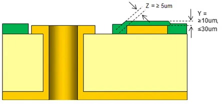
PCB solder mask thickness standard
Solder mask thickness is standardized according to IPC-SM-840C specifications:
-
Class 1 (General Electronic Products): No minimum thickness requirement
-
Class 2 (Dedicated Service Electronic Products): Minimum 10μm
-
Class 3 (High-Reliability Electronic Products): Minimum 18μm
Typically, the solder mask thickness is:
-
≥10μm over traces
-
≥5μm on trace edges
Additionally, solder mask materials SSmust comply with UL94V-0 flammability standards to ensure flame resistance.
Functions of PCB solder mask
1. Prevent short circuit and leakage
- The lines on the PCB are dense and the spacing is small. If there is no protection of solder mask, adjacent lines may cause short circuit or leakage due to accidental contact. solder mask covers the area where soldering is not required, forming an insulation barrier, which effectively avoids this situation.
2. Provide insulation protection
- Electronic equipment will be subject to various electromagnetic interference and voltage fluctuations during operation. Good insulation performance is essential to ensure the normal operation of the circuit. PCB solder mask can isolate the circuit from the external environment, prevent moisture, dust, corrosive gases, etc. from entering, thereby improving the insulation resistance and voltage resistance of the PCB, and ensuring the stability and reliability of electronic equipment.
3. Protect the circuit from mechanical damage
- During the manufacturing, assembly and use of PCBs, they will inevitably be subject to various mechanical stresses, such as plugging and unplugging components, collisions during transportation, etc. solder mask can provide a tough protective film for the circuit, reduce the impact of mechanical damage on the circuit, and extend the service life of the PCB.
4. Improve soldering quality
- solder mask clearly defines the soldering area, making the soldering process more accurate and efficient. It can prevent solder from flowing in unnecessary areas, reduce the occurrence of soldering defects such as cold soldering and bridging, and improve the assembly quality and production efficiency of PCBs.
5. Enhance corrosion resistance
- Electronic equipment may be exposed to various corrosive substances such as acids, alkalis, salts, etc. in the use environment. solder mask can prevent these corrosive substances from directly contacting the metal circuits on the surface of the PCB, thereby delaying the corrosion and oxidation of the circuits and improving the corrosion resistance and service life of the PCB.
6. Optimize heat dissipation performance
- Some types of PCB solder mask have certain thermal conductivity, which can help components on the PCB dissipate heat and improve the working stability and reliability of electronic equipment.
7. Beautify the appearance
- In addition to its functional role, PCB solder mask can also provide a beautiful appearance for the PCB. solder masks of different colors and patterns can make the PCB look more neat and professional, and enhance the market competitiveness of the product.
Types of PCB Solder Masks
Liquid Photoimageable (LPI) Solder Mask
LPI is the most widely adopted method for modern PCBs. It’s applied in liquid form, photo-imaged with UV light, and developed chemically.
Detailed breakdown: Comprehensive Introduction to LPI Solder Mask in PCB Manufacturing
Dry Film Solder Mask
Dry film masks are laminated onto the board and exposed to UV light. While less common today, they’re still used in high-precision applications.
Peelable Solder Mask
Used in temporary soldering or protection zones, especially during wave soldering.
Application Process of Solder Mask
Standard application steps include:
-
PCB cleaning
-
Coating the solder mask layer (via spray, curtain, or screen printing)
-
Pre-baking (optional)
-
Photo-imaging (for LPI)
-
Development (etching away unexposed mask)
-
Final curing (thermal or UV)
For more on the process: Solder Mask Application: Best Practices for Durability
Design Considerations: Solder Mask Bridge
A solder mask bridge is a thin strip of solder mask material intentionally left between two exposed pads on a PCB. It acts as an insulating barrier to prevent excess solder from flowing and forming bridges between adjacent pads—particularly important for fine-pitch components such as ICs.
However, designing solder mask bridges requires careful consideration of several factors:
-
Pad Spacing: If pads are too close, it may not be possible to form an effective bridge, increasing the risk of solder shorts.
-
Minimum Mask Web Width: PCB fabrication processes have limitations on how narrow the solder mask web can be without peeling or breaking.
-
Alignment Tolerance: The photolithographic process must be precise enough to ensure that the bridge aligns with the space between pads.
Too wide a bridge may mask part of the pad, affecting solderability, while too narrow a bridge may peel off during assembly.
Paste Mask vs. Solder Mask: What’s the Difference?
Despite similar names, paste mask and solder mask serve entirely different purposes in PCB manufacturing:
-
Solder Mask is a protective coating applied over the PCB surface (except pads) to prevent oxidation and solder bridging. It is part of the bare PCB fabrication process.
-
Paste Mask (also called stencil layer or paste layer) defines the areas where solder paste should be deposited during the assembly process. It is used to create a stainless steel stencil that matches the pad openings, enabling precise placement of solder paste.
| Feature | Solder Mask | Paste Mask |
|---|---|---|
| Purpose | Prevent solder bridging, oxidation, and contamination | Define where solder paste is applied for surface-mount components |
| Layer | Applied as a protective coating over the PCB | Used to create a stencil for reflow soldering |
| Material | Epoxy or photoimageable polymer | CAD-generated opening data for stainless-steel stencils |
| Appearance | Green, red, blue, black, etc. | Invisible on finished PCB |
Confused between the two? Get more clarity here: What Are the Differences Between Paste Mask and Solder Mask?
High-Frequency PCBs and Solder Mask Materials
In high-frequency applications (such as RF, microwave, or 5G PCBs), solder mask material selection becomes crucial due to its influence on signal integrity. Traditional solder masks are often optimized for mechanical and chemical protection, but not for high-speed signal performance.
Why Solder Mask Matters in High-Frequency PCBs:
-
Dielectric Constant (Dk): Standard solder masks have relatively high Dk (~4.0), which can introduce impedance mismatches at GHz frequencies.
-
Loss Tangent (Df): High Df contributes to signal attenuation, especially in edge-coupled differential pairs.
-
Thickness Variability: Uneven solder mask thickness can alter the impedance of controlled trace geometries.
Recommended Solder Mask Materials:
-
Low-Dk Liquid Photoimageable (LPI) Masks: Designed for high-frequency boards, these masks reduce signal loss and impedance variation.
-
Liquid Crystal Polymer (LCP): Offers extremely low Dk and Df, ideal for millimeter-wave frequencies.
-
Polyimide-based solder masks: Often used for flexible or RF circuits due to excellent thermal and electrical properties.
ALLPCB works closely with trusted material suppliers to offer solder mask materials specifically optimized for high-frequency performance. We ensure precise coating control, consistent thickness, and compatibility with Rogers, PTFE, or other advanced RF substrates.
Explore more on this topic here: Solder Mask Materials for High-Frequency PCBs: Minimizing Signal Loss
Conclusion: The Evolving Role of Solder Masks in PCB Technology
As electronics continue to miniaturize and diversify, solder mask technology will also evolve. From high-frequency materials to finer imaging and automation-friendly processes, the demand for precision and performance in solder masking is ever increasing.
For design engineers and PCB manufacturers alike, understanding solder mask properties and applications is key to delivering robust, reliable, and scalable circuit boards.
Stay updated with ALLPCB for professional manufacturing support and continuous knowledge sharing in PCB technology.


