 ALLPCB


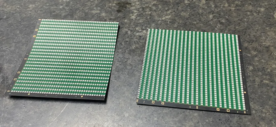
Panel size plays a critical role in PCB warpage, a common issue that can disrupt the manufacturing and assembly process of printed circuit boards. Larger panels often lead to increased stress during panelization, while improper material selection or board thickness can worsen bending. In this comprehensive guide, we’ll explore how panel size impacts PCB warpage, the causes behind it, and practical techniques for preventing PCB bending. Whether you're dealing with panelization stress or seeking the right material for panel stability, this blog will provide actionable insights to ensure your boards remain flat and functional.
Understanding PCB Warpage and Its Connection to Panel Size
PCB warpage refers to the unwanted bending or deformation of a printed circuit board, which can cause issues like poor solder joint formation, inaccurate component placement, and even complete assembly failure. One of the key factors influencing warpage is the panel size used during manufacturing. When multiple PCBs are arranged on a single panel for efficient production—a process known as panelization—the size and design of that panel can introduce stresses that lead to bending.
Larger panels, while cost-effective for mass production, often experience uneven thermal expansion and mechanical stress during processes like reflow soldering. For instance, a panel measuring 18 x 24 inches may undergo significant temperature gradients across its surface, causing one area to expand or contract more than another. This imbalance directly contributes to warpage. Understanding the relationship between panel size and these stresses is the first step in tackling the problem.
Key Causes of Warpage in PCB Assembly Process
To address PCB warpage, it’s important to identify the root causes, especially those tied to panel size and assembly processes. Below are the primary factors contributing to warpage:
- Panelization Stress: During panelization, multiple boards are connected on a single panel using tabs or breakaway rails. Larger panels create more stress at these connection points due to uneven weight distribution or thermal expansion, leading to bending.
- Thermal Imbalance: In processes like reflow soldering, different parts of a large panel may heat or cool at varying rates. For example, a panel with a high component density on one side may retain more heat, causing uneven expansion and warpage.
- Board Thickness and Panel Size Relation: Thinner boards are more prone to bending, especially on larger panels. A 0.8mm thick board on a 20 x 20-inch panel is far more likely to warp than a 1.6mm thick board on the same panel due to reduced structural rigidity.
- Material Selection for Panel Stability: The choice of substrate material, such as FR-4 or high-Tg laminates, impacts how a panel responds to heat and stress. Lower-quality materials may not withstand the demands of larger panel sizes, leading to deformation.
- Copper Distribution: Uneven copper distribution across a PCB design can cause localized stress. On a large panel, this effect is magnified as areas with dense copper traces resist thermal expansion more than areas with less copper.
By recognizing these causes, manufacturers can take targeted steps to minimize warpage risks associated with panel size during PCB assembly.
How Panel Size Directly Impacts PCB Warpage
The size of a panel directly influences the level of mechanical and thermal stress a PCB experiences during manufacturing. Here’s how:
1. Larger Panels and Thermal Gradients
Larger panels, such as those exceeding 18 x 24 inches, are more susceptible to temperature differences across their surface during soldering or lamination. For instance, if the center of the panel heats up faster than the edges, the material will expand unevenly, resulting in a bowed or twisted shape. This issue is less pronounced in smaller panels (e.g., 9 x 12 inches) where heat distribution is more uniform.
2. Mechanical Stress from Panel Weight
A larger panel naturally weighs more and can sag or bend under its own weight during handling or processing. This mechanical stress is especially problematic for thinner boards (below 1.2mm), as they lack the structural strength to resist deformation over a wide area.
3. Panelization Layout Challenges
When arranging multiple PCBs on a large panel, the layout must balance stress points. Poorly designed panelization, such as placing boards too close to the panel edges or using insufficient support tabs, increases the risk of warpage. Larger panels often require more complex layouts, amplifying these risks.
Board Thickness and Panel Size Relation: Finding the Balance
The relationship between board thickness and panel size is a critical factor in preventing PCB bending. Thinner boards, while lightweight and cost-effective, are more prone to warpage on larger panels due to their lower mechanical strength. Here are some guidelines based on common industry standards:
- For small panels (under 12 x 12 inches), a board thickness of 0.8mm to 1.0mm is often sufficient to avoid significant warpage.
- For medium panels (12 x 18 inches), a thickness of 1.2mm to 1.6mm provides better stability against thermal and mechanical stress.
- For large panels (over 18 x 24 inches), opt for a thickness of 1.6mm or higher to ensure the board can withstand handling and processing without bending.
Choosing the right thickness based on panel size can significantly reduce warpage risks. Additionally, reinforcing thinner boards with support structures during panelization can help maintain flatness on larger panels.
Material Selection for Panel Stability
The choice of material is another crucial aspect of preventing PCB warpage, especially when dealing with varying panel sizes. Different substrates have unique properties that affect how they handle thermal and mechanical stress. Consider these options:
- FR-4: A widely used material with good thermal stability for small to medium panels. However, standard FR-4 may struggle with warpage on larger panels under high heat (above 130°C).
- High-Tg FR-4: With a glass transition temperature (Tg) of 150°C or higher, this variant offers better resistance to thermal stress, making it ideal for larger panels exposed to reflow soldering.
- Polyimide: Known for excellent thermal stability (Tg above 200°C), polyimide is a premium choice for high-reliability applications on large panels, though it comes at a higher cost.
- Metal-Core PCBs: For applications requiring heat dissipation, metal-core materials like aluminum provide added rigidity, reducing warpage risks on larger panels.
Selecting a material with the right thermal and mechanical properties for your panel size can make a significant difference in maintaining board flatness.
Preventing PCB Bending: Practical Techniques for Warpage Control
Now that we’ve covered the causes and impacts of PCB warpage related to panel size, let’s dive into actionable techniques to prevent bending and ensure a smooth assembly process.
1. Optimize Panel Size and Layout
Whenever possible, use smaller panels for thinner boards to minimize thermal gradients and mechanical stress. If large panels are necessary for cost efficiency, ensure an even distribution of PCBs across the panel. Adding dummy boards or support structures near the edges can balance stress and reduce warpage.
2. Balance Copper Distribution
Design your PCB with balanced copper layers on both sides to avoid uneven thermal expansion. For example, if one side of the board has a dense copper ground plane, replicate a similar pattern on the opposite side to maintain symmetry. This is especially important for larger panels where imbalances are more noticeable.
3. Use Pre-Baking and Controlled Cooling
Pre-baking PCBs before assembly removes moisture that can cause uneven expansion during soldering. Additionally, implement controlled cooling after reflow soldering to prevent rapid temperature drops that lead to warpage. For large panels, cooling rates of 2-3°C per second are often recommended.
4. Employ Support Fixtures During Assembly
Using pallets or fixtures during reflow soldering can hold the panel flat and prevent bending. These support structures are particularly effective for large panels or thinner boards (below 1.2mm), ensuring uniform heat distribution and minimizing mechanical stress.
5. Adjust Reflow Profiles for Panel Size
Tailor the reflow soldering temperature profile to the specific panel size. For larger panels, a slower ramp-up rate (e.g., 1.5°C per second) helps achieve uniform heating, reducing the risk of thermal stress. Monitor peak temperatures to stay within the material’s limits, typically below 260°C for standard FR-4.
Advanced Tips for Managing Panelization Stress
Panelization stress is a major contributor to warpage, especially on larger panels. Here are some advanced strategies to manage this issue:
- Strategic Tab Placement: Place breakaway tabs or V-scoring lines at regular intervals to distribute stress evenly. Avoid placing tabs too close to critical components, as this can cause localized bending.
- Add Stress Relief Slots: Incorporate small slots or perforations near the panel edges to relieve mechanical stress during handling and processing.
- Simulate Panel Behavior: Use simulation software to predict warpage based on panel size, material, and layout. This can help identify potential issues before manufacturing begins, saving time and resources.
Conclusion: Mastering PCB Warpage Control with Panel Size Awareness
Panel size has a profound impact on PCB warpage, influencing everything from thermal stress to mechanical stability. By understanding the relationship between panel size, board thickness, and material selection, manufacturers can take proactive steps to prevent bending and ensure high-quality assembly outcomes. From optimizing panel layouts to using the right materials and support fixtures, the techniques outlined in this guide offer practical solutions for tackling warpage causes in the PCB assembly process.
Implementing these strategies not only improves the reliability of your boards but also reduces costly defects and rework. Whether you’re working with small or large panels, a thoughtful approach to panelization stress and warpage prevention will keep your PCBs flat, functional, and ready for the demands of modern electronics.


