 ALLPCB


Designing a printed circuit board (PCB) that performs reliably and efficiently starts with a solid foundation: power and ground planes. These planes are critical for providing stable power distribution, reducing noise, and ensuring signal integrity. Whether you're a beginner or an experienced engineer, understanding how to implement power and ground planes in PCB design is essential for creating high-quality boards. In this comprehensive guide, we’ll dive into the best practices for power plane and ground plane implementation, offering actionable tips to optimize your PCB design process using industry-standard tools like Cadence software.
Why Power and Ground Planes Matter in PCB Design
Power planes and ground planes serve as the backbone of any PCB design. A power plane delivers a consistent voltage to components, while a ground plane provides a common reference point for signals and helps minimize electromagnetic interference (EMI). Together, they ensure low impedance paths, reduce noise, and improve overall circuit performance. Without proper implementation, you risk issues like voltage drops, signal distortion, or even complete system failure.
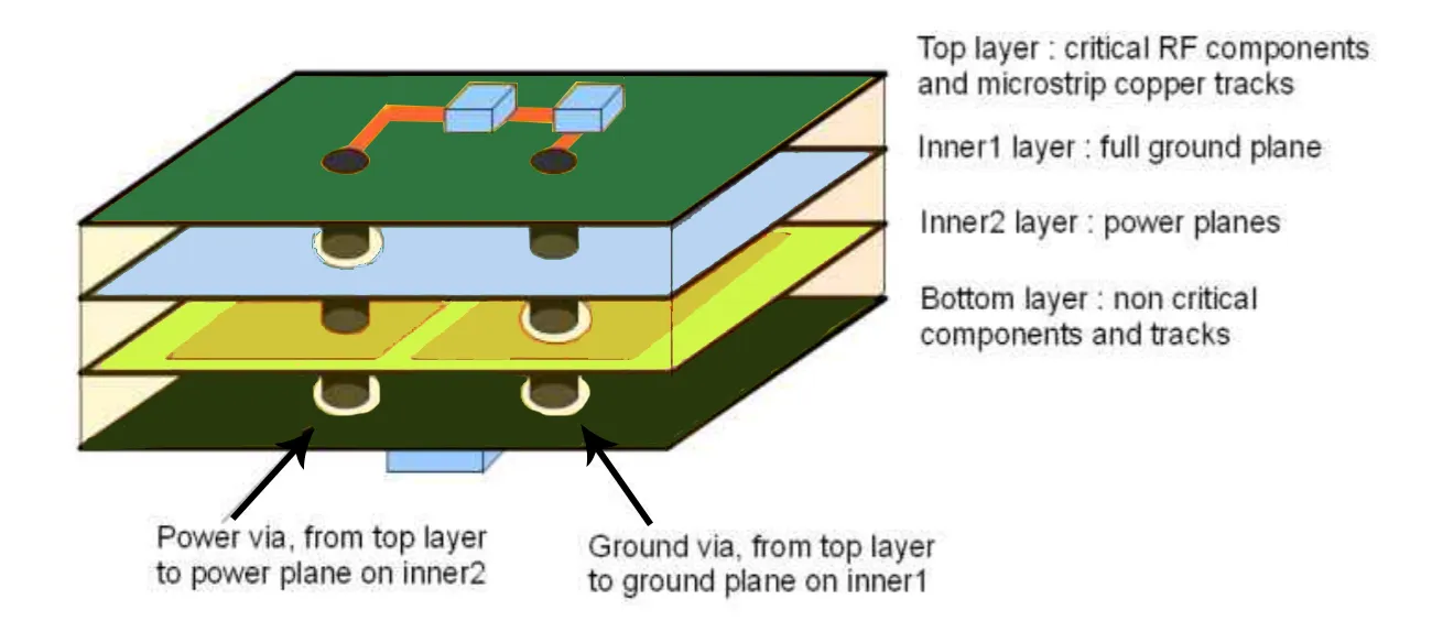
In modern multi-layer PCB designs, these planes are often dedicated layers within the board stackup. For instance, a 4-layer PCB might have the top and bottom layers for signals and components, with the inner layers dedicated to power and ground. This setup not only saves space but also enhances the board's electrical performance by keeping return paths short and direct.
Key Benefits of Power and Ground Planes
- Stable Power Distribution: Power planes ensure uniform voltage across the board, preventing drops that can affect component performance.
- Reduced EMI: Ground planes act as a shield, minimizing interference between signals and external sources.
- Improved Signal Integrity: A well-designed ground plane provides a low-impedance return path for high-speed signals, reducing crosstalk and reflections.
- Thermal Management: Large copper planes help dissipate heat, protecting compone
- nts from overheating.
Best Practices for Power Plane Design in PCBs
Implementing a power plane effectively requires careful planning during the design phase. Below are some best practices to follow for optimal power distribution and performance in your PCB design.
1. Dedicate a Layer for Power Distribution
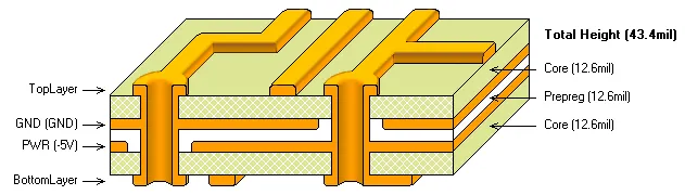
In multi-layer boards, reserve an entire layer for the power plane whenever possible. This ensures a low-impedance path for current flow, minimizing voltage drops. For example, in a 6-layer stackup, you might place the power plane on layer 2, directly below the top signal layer, to keep power delivery close to components. If a full layer isn’t feasible, split the plane into sections for different voltage levels (e.g., 3.3V and 5V), but avoid overlapping to prevent interference.
2. Use Proper Decoupling Capacitors
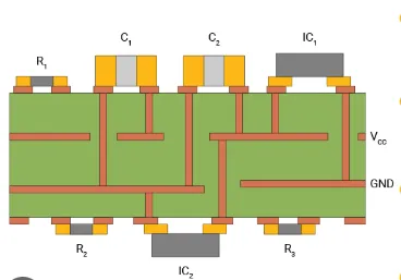
Decoupling capacitors are essential for stabilizing voltage on the power plane, especially in high-speed designs. Place these capacitors close to the power pins of integrated circuits (ICs) to filter out noise. A common guideline is to use a mix of capacitor values, such as 0.1 μF and 1 μF, to cover a range of frequencies. Ensure the capacitors connect directly to the power and ground planes through vias for the shortest possible path.
3. Minimize Power Plane Splits
Splitting a power plane to accommodate multiple voltages can create discontinuities that disrupt current flow and increase impedance. If splits are necessary, keep them minimal and ensure that signal traces don’t cross over the split, as this can lead to signal integrity issues. Use stitching capacitors across splits to maintain a continuous return path if needed.
Best Practices for Ground Plane Design in PCBs
A ground plane is just as crucial as a power plane, providing a stable reference for signals and a return path for currents. Here are some key practices to ensure your ground plane enhances your PCB design.
1. Use a Continuous Ground Plane
Whenever possible, dedicate an entire layer to a continuous ground plane without splits or cuts. A solid ground plane reduces loop inductance and provides a consistent return path for signals, which is critical for high-speed designs operating at frequencies above 100 MHz. Breaks in the ground plane can force return currents to take longer paths, increasing EMI and noise.
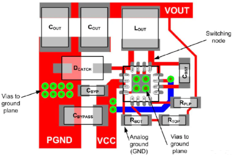
2. Place Ground Vias Strategically
Ground vias connect components and signal traces to the ground plane, ensuring a low-impedance return path. Place these vias close to signal transitions, especially for high-speed signals, to minimize loop areas. For example, in a design with differential pairs, place ground vias adjacent to signal vias to maintain signal integrity and reduce crosstalk.
3. Avoid Routing Signals Over Ground Plane Gaps
Routing signal traces over gaps or splits in the ground plane disrupts the return path, leading to signal distortion and increased EMI. If a split is unavoidable, ensure the return path remains intact by adding stitching vias or using a different layer for the signal trace. Tools like Cadence software can help visualize and avoid such issues during the layout phase.
Related Reading: Mastering PCB Inner Layer Stackup: Optimizing Power and Ground Planes
Optimizing Power and Ground Planes Together
While power and ground planes serve distinct purposes, they work best when designed as a cohesive system. Here are tips to optimize their combined performance in your PCB design.
1. Position Power and Ground Planes Adjacent to Each Other
In a multi-layer stackup, place the power and ground planes on adjacent layers to create a natural capacitance between them. This capacitance helps filter out high-frequency noise and stabilizes voltage. For instance, in a 4-layer board, place the ground plane on layer 2 and the power plane on layer 3, with signal layers on the top and bottom. The typical spacing between these planes is around 4-10 mils (0.1-0.25 mm) to maximize capacitance while maintaining manufacturability.
2. Use Multiple Ground Planes for High-Speed Designs
For complex or high-speed designs, consider using multiple ground planes to provide additional shielding and return paths. This is especially useful in boards with mixed-signal components, where analog and digital grounds need separation to prevent noise coupling. However, ensure these grounds connect at a single point (star grounding) to avoid ground loops.
3. Manage Thermal Dissipation
Power and ground planes can also aid in thermal management by spreading heat across the board. Use thermal vias to connect heat-generating components to these planes, ensuring efficient heat dissipation. For high-power designs, increase the copper thickness of the planes (e.g., 2 oz/ft2 instead of 1 oz/ft2) to handle higher currents and improve thermal conductivity.
Leveraging Cadence Tools for Power and Ground Plane Design
Modern PCB design software, such as Cadence, offers powerful features to streamline the implementation of power and ground planes. These tools help engineers visualize, simulate, and optimize their designs for maximum performance. Here’s how you can use such software to enhance your PCB design process.
1. Define Plane Layers Easily
Cadence software allows you to designate specific layers as power or ground planes during the stackup design phase. You can assign net names (e.g., VCC or GND) to these layers, ensuring automatic connections to corresponding component pins. This feature reduces manual errors and speeds up the layout process.
2. Simulate Power Integrity
Power integrity analysis tools within Cadence help identify potential issues like voltage drops or excessive noise on the power plane. By simulating current distribution and impedance, you can adjust plane shapes or add decoupling capacitors before fabrication. For example, simulations might reveal a voltage drop of 0.2V at a specific IC, prompting design adjustments to ensure stable operation.
3. Automate Ground Via Placement
High-speed design often requires precise placement of ground vias to maintain signal integrity. Cadence tools can automate via stitching around critical areas, ensuring consistent return paths without manual effort. This is particularly useful for large designs with hundreds of vias.
Related Reading: The Ultimate Guide to PCB Ground Planes: Boost Signal Integrity and Reduce EMI
Common Mistakes to Avoid in Power and Ground Plane Design
Even with the best tools, mistakes in power and ground plane implementation can lead to costly redesigns. Here are some pitfalls to watch out for in your PCB design.
1. Insufficient Decoupling
Failing to use enough decoupling capacitors or placing them too far from ICs can result in voltage fluctuations and noise. As a rule of thumb, place at least one 0.1 μF capacitor per power pin for high-speed ICs, within 100 mils (2.54 mm) of the pin.
2. Overlapping Power and Ground Splits
Overlapping splits between power and ground planes can create unintended coupling and noise. Always align splits carefully or avoid them altogether by using separate layers for different voltages.
3. Neglecting Return Paths
Ignoring the return path for high-speed signals can lead to EMI and signal degradation. Ensure that every signal trace has a nearby ground plane or via to complete the current loop, especially for signals switching at speeds above 50 MHz.
Conclusion: Building Better PCBs with Power and Ground Planes
Implementing power and ground planes effectively is a cornerstone of successful PCB design. By following best practices—such as dedicating layers to planes, minimizing splits, using decoupling capacitors, and leveraging tools like Cadence software—you can create boards that deliver reliable performance and minimal noise. Whether you’re working on a simple 2-layer board or a complex high-speed design, a well-planned approach to power plane and ground plane implementation will save time, reduce errors, and improve the overall quality of your project.
Start by reviewing your current designs with these guidelines in mind. Pay close attention to layer stackups, via placement, and simulation results to ensure your power and ground planes are optimized. With these strategies, you’ll be well on your way to mastering PCB design and achieving superior results in every project.


