Working with 8-layer printed circuit boards (PCBs) requires precision and care to ensure safety and prevent accidents. These complex boards, often used in high-speed and high-density electronic designs, come with unique challenges. By following safe practices in handling, soldering, and disposal, you can protect yourself and your equipment. In this detailed guide, we’ll cover essential electronics safety tips, soldering safety precautions, PCB handling safety, component disposal, and electrical safety to help you work confidently with 8-layer PCBs.
Why Safety Matters with 8-Layer PCBs
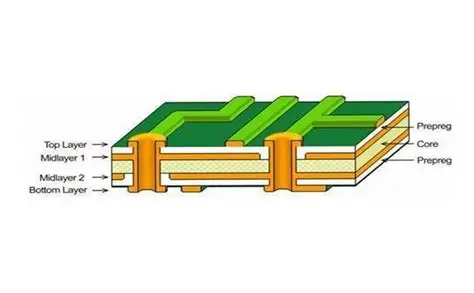
8-layer PCBs are advanced boards with multiple layers of conductive material, often used in applications like telecommunications, medical devices, and aerospace technology. These boards manage high-speed signals (often exceeding 1 GHz) and require precise impedance control (typically around 50 ohms for high-frequency designs). However, their complexity increases risks such as electrical shocks, burns from soldering, and damage to sensitive components if mishandled. Prioritizing safety not only protects you but also ensures the integrity of the board, avoiding costly rework or failures.

Key Electronics Safety Tips for Working with 8-Layer PCBs
Safety in electronics starts with a solid understanding of the risks involved. Here are practical tips to minimize hazards when working with multilayer boards:
- Always Power Down Equipment: Before touching any PCB or connected components, ensure all power sources are disconnected. Even low voltages can cause shocks or short circuits in densely packed 8-layer designs.
- Use Insulated Tools: Opt for tools with insulated handles to prevent accidental contact with live circuits. This is critical when probing or adjusting components on a board with tight spacing.
- Wear Protective Gear: Safety glasses protect your eyes from solder splashes or debris, while heat-resistant gloves can shield your hands during soldering tasks.
- Work in a Well-Ventilated Area: Fumes from soldering or cleaning solvents can be harmful. Ensure your workspace has proper ventilation to avoid inhaling toxic substances.
Following these electronics safety tips creates a secure environment, especially when dealing with the intricate designs of 8-layer PCBs.
Soldering Safety Precautions for 8-Layer PCBs
Soldering is a critical step in assembling or repairing PCBs, but it comes with risks like burns and exposure to harmful fumes. With 8-layer PCBs, precision is even more important due to the tight component spacing and multiple internal layers. Here are key soldering safety precautions:
- Use the Right Soldering Iron: Choose a soldering iron with adjustable temperature control (typically 300-350°C for most PCB work) to avoid overheating delicate components or damaging internal layers. Overheating can cause delamination in multilayer boards.
- Keep Your Workspace Clean: Remove clutter to prevent accidental burns or spills. A clean area also helps you focus on precise soldering, which is essential for small pads on 8-layer PCBs.
- Avoid Lead Exposure: Many solders contain lead, which is toxic. Use lead-free solder when possible, and wash your hands thoroughly after soldering to avoid ingestion or skin contact.
- Use a Fume Extractor: Soldering releases fumes that can irritate your lungs. A fume extractor or working near an exhaust fan helps remove these harmful particles from your breathing zone.
- Handle Hot Equipment with Care: Always place the soldering iron in a stand when not in use. Never touch the tip, as it can cause severe burns.
By adhering to these soldering safety precautions, you reduce the risk of injury and ensure high-quality connections on your 8 layer PCB.

PCB Handling Safety: Protecting Yourself and the Board
Handling an 8-layer PCB requires extra care due to its complexity and sensitivity to physical and electrostatic damage. Improper handling can lead to cracked boards, damaged traces, or component failure. Follow these PCB handling safety practices:
- Wear Anti-Static Wrist Straps: Electrostatic discharge (ESD) can destroy sensitive components on an 8-layer PCB. Always wear a grounded anti-static wrist strap and work on an anti-static mat to prevent static buildup.
- Hold by the Edges: Avoid touching the surface of the PCB, especially the pads and components. Hold the board by its edges to prevent oils from your skin from contaminating the surface or causing shorts.
- Store Properly: When not in use, store PCBs in anti-static bags or containers to protect them from dust, moisture, and ESD. This is especially important for 8-layer boards with exposed vias or fine traces.
- Avoid Excessive Force: Don’t bend or twist the PCB, as multilayer boards are more prone to internal layer separation. Even minor stress can disrupt signal integrity, especially in high-speed designs.
These PCB handling safety tips help preserve the functionality of your 8-layer PCB while keeping you safe from potential hazards like static shocks.
Component Disposal: Handling Electronic Waste Safely
Disposing of components and materials from 8-layer PCBs is often overlooked but is crucial for safety and environmental responsibility. Improper disposal can lead to exposure to toxic substances or legal penalties. Here’s how to manage component disposal safely:
- Separate Electronic Waste: Don’t throw PCB components or scraps in regular trash. Materials like capacitors, resistors, and solder may contain hazardous substances such as lead or mercury.
- Use Authorized E-Waste Centers: Take discarded components and damaged PCBs to certified e-waste recycling facilities. These centers ensure safe processing and prevent harmful chemicals from leaching into the environment.
- Handle Damaged Components Carefully: Broken components, like capacitors, can leak toxic electrolytes. Wear gloves and place them in sealed containers before disposal to avoid contact with skin or eyes.
- Follow Local Regulations: Different regions have specific rules for electronic waste disposal. Familiarize yourself with local guidelines to ensure compliance and avoid fines.
Proper component disposal not only protects the environment but also prevents health risks associated with toxic materials often found in electronics.

Electrical Safety: Minimizing Risks with 8-Layer PCBs
Electrical safety is paramount when working with any PCB, especially 8-layer designs that often handle higher voltages and currents in compact spaces. A single misstep can lead to shocks, short circuits, or fires. Keep these electrical safety practices in mind:
- Check for Live Circuits: Use a multimeter to verify that no voltage is present before working on the PCB. Even residual power in capacitors (often rated at 10-100 μF in such designs) can cause a shock.
- Insulate Exposed Conductors: If any wires or traces are exposed during testing or repair, cover them with electrical tape or heat-shrink tubing to prevent accidental contact.
- Limit High-Voltage Testing: When testing high-speed circuits on an 8-layer PCB, use low-voltage settings first (e.g., 3.3V or 5V) before ramping up to operational levels (sometimes up to 12V or higher). This minimizes the risk of arcing or component failure.
- Ground Your Equipment: Ensure all test equipment, like oscilloscopes or power supplies, is properly grounded to avoid creating dangerous voltage differences that could lead to shocks.
By prioritizing electrical safety, you can prevent accidents and maintain the reliability of your 8-layer PCB during testing and operation.
Creating a Safe Workspace for PCB Work
Beyond specific practices, your overall workspace setup plays a big role in preventing accidents. Here’s how to create a safe environment for working with 8-layer PCBs:
- Organize Tools and Materials: Keep tools, components, and documentation in designated spots to avoid clutter. A tidy workspace reduces the chance of knocking over equipment or misplacing critical parts.
- Ensure Proper Lighting: Good lighting helps you see fine details on an 8-layer PCB, reducing the risk of errors during soldering or inspection. Use adjustable desk lamps for focused illumination.
- Install Emergency Equipment: Keep a fire extinguisher rated for electrical fires nearby, as well as a first-aid kit for minor injuries like burns or cuts.
- Label Hazardous Areas: If you’re working with high-voltage setups or chemicals for PCB cleaning, label these areas clearly to alert others and remind yourself of potential dangers.
A well-prepared workspace complements the safety practices outlined above, creating a secure environment for handling complex multilayer boards.
Common Mistakes to Avoid with 8-Layer PCBs
Even with the best intentions, certain mistakes can compromise safety and board performance. Be mindful of these common pitfalls:
- Ignoring ESD Precautions: Skipping anti-static measures can instantly damage components, especially on densely packed 8-layer PCBs where a single discharge can affect multiple layers.
- Overheating During Soldering: Applying too much heat (above 400°C for prolonged periods) can lift pads or damage internal traces, ruining the board’s signal integrity.
- Improper Storage: Leaving PCBs exposed to humidity (above 60% relative humidity) or dust can lead to corrosion or contamination, affecting performance in high-frequency applications.
- Neglecting Disposal Rules: Tossing electronic waste in regular bins risks environmental harm and potential fines, as many PCB materials are classified as hazardous.
Avoiding these mistakes ensures both your safety and the longevity of your 8-layer PCB projects.
Conclusion: Building a Culture of Safety with 8-Layer PCBs
Working with 8-layer PCBs offers incredible opportunities for advanced electronic designs, but it demands a strong commitment to safety. By following the electronics safety tips, soldering safety precautions, PCB handling safety practices, proper component disposal methods, and electrical safety guidelines outlined in this guide, you can prevent accidents and protect your work. A safe approach not only keeps you out of harm’s way but also ensures the quality and reliability of your multilayer boards. Whether you’re soldering tiny components or testing high-speed circuits, prioritize safety at every step to achieve the best results.
 ALLPCB


